Chapter 1 · Semiconductor Diodes
Vector reconstruction of the original PDF. Text remains searchable/selectable through the aligned HTML text layer.

CHAPTER OBJECTIVES●● Become aware of the general characteristics of three important semiconductormaterials: Si, Ge, GaAs.● Understand conduction using electron and hole theory.● Be able to describe the difference between n - and p -type materials.● Develop a clear understanding of the basic operation and characteristics of a diode inthe no-bias, forward-bias, and reverse-bias regions.● Be able to calculate the dc, ac, and average ac resistance of a diode from thecharacteristics.● Understand the impact of an equivalent circuit whether it is ideal or practical.● Become familiar with the operation and characteristics of a Zener diode andlight- emitting diode.1.1INTRODUCTION●One of the noteworthy things about this field, as in many other areas of technology, is howlittle the fundamental principles change over time. Systems are incredibly smaller, currentspeeds of operation are truly remarkable, and new gadgets surface every day, leaving us towonder where technology is taking us. However, if we take a moment to consider that themajority of all the devices in use were invented decades ago and that design techniquesappearing in texts as far back as the 1930s are still in use, we realize that most of what wesee is primarily a steady improvement in construction techniques, general characteristics,and application techniques rather than the development of new elements and fundamen-tally new designs. The result is that most of the devices discussed in this text have beenaround for some time, and that texts on the subject written a decade ago are still good ref-erences with content that has not changed very much. The major changes have been in theunderstanding of how these devices work and their full range of capabilities, and inimproved methods of teaching the fundamentals associated with them. The benefit of allthis to the new student of the subject is that the material in this text will, we hope, havereached a level where it is relatively easy to grasp and the information will have applica-tion for years to come.The miniaturization that has occurred in recent years leaves us to wonder about its limits.Complete systems now appear on wafers thousands of times smaller than the single elementof earlier networks. The first integrated circuit (IC) was developed by Jack Kilby whileworking at Texas Instruments in 1958 ( Fig. 1.1 ). Today, the Intel ® Core TM i7 Extreme1Semiconductor Diodes1
textbook p. 1PDF p. 22
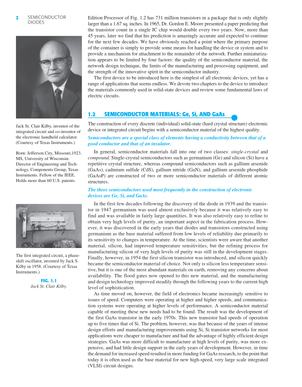
Edition Processor of Fig. 1.2 has 731 million transistors in a package that is only slightlylarger than a 1.67 sq. inches. In 1965, Dr. Gordon E. Moore presented a paper predicting thatthe transistor count in a single IC chip would double every two years. Now, more than45 years, later we find that his prediction is amazingly accurate and expected to continuefor the next few decades. We have obviously reached a point where the primary purposeof the container is simply to provide some means for handling the device or system and toprovide a mechanism for attachment to the remainder of the network. Further miniaturiza-tion appears to be limited by four factors: the quality of the semiconductor material, thenetwork design technique, the limits of the manufacturing and processing equipment, andthe strength of the innovative spirit in the semiconductor industry.The first device to be introduced here is the simplest of all electronic devices, yet has arange of applications that seems endless. We devote two chapters to the device to introducethe materials commonly used in solid-state devices and review some fundamental laws ofelectric circuits.1.2SEMICONDUCTOR MATERIALS: Ge, Si, AND GaAs ●The construction of every discrete (individual) solid-state (hard crystal structure) electronicdevice or integrated circuit begins with a semiconductor material of the highest quality.Semiconductors are a special class of elements having a conductivity between that of agood conductor and that of an insulator.In general, semiconductor materials fall into one of two classes: single-crystal andcompound. Single-crystal semiconductors such as germanium (Ge) and silicon (Si) have arepetitive crystal structure, whereas compound semiconductors such as gallium arsenide(GaAs), cadmium sulfide (CdS), gallium nitride (GaN), and gallium arsenide phosphide(GaAsP) are constructed of two or more semiconductor materials of different atomicstructures.The three semiconductors used most frequently in the construction of electronicdevices are Ge, Si, and GaAs.In the first few decades following the discovery of the diode in 1939 and the transis-tor in 1947 germanium was used almost exclusively because it was relatively easy tofind and was available in fairly large quantities. It was also relatively easy to refine toobtain very high levels of purity, an important aspect in the fabrication process. How-ever, it was discovered in the early years that diodes and transistors constructed usinggermanium as the base material suffered from low levels of reliability due primarily toits sensitivity to changes in temperature. At the time, scientists were aware that anothermaterial, silicon, had improved temperature sensitivities, but the refining process formanufacturing silicon of very high levels of purity was still in the development stages.Finally, however, in 1954 the first silicon transistor was introduced, and silicon quicklybecame the semiconductor material of choice. Not only is silicon less temperature sensi-tive, but it is one of the most abundant materials on earth, removing any concerns aboutavailability. The flood gates now opened to this new material, and the manufacturingand design technology improved steadily through the following years to the current highlevel of sophistication.As time moved on, however, the field of electronics became increasingly sensitive toissues of speed. Computers were operating at higher and higher speeds, and communica-tion systems were operating at higher levels of performance. A semiconductor materialcapable of meeting these new needs had to be found. The result was the development ofthe first GaAs transistor in the early 1970s. This new transistor had speeds of operationup to five times that of Si. The problem, however, was that because of the years of intensedesign efforts and manufacturing improvements using Si, Si transistor networks for mostapplications were cheaper to manufacture and had the advantage of highly efficient designstrategies. GaAs was more difficult to manufacture at high levels of purity, was more ex-pensive, and had little design support in the early years of development. However, in timethe demand for increased speed resulted in more funding for GaAs research, to the point thattoday it is often used as the base material for new high-speed, very large scale integrated(VLSI) circuit designs.SEMICONDUCTORDIODES2Jack St. Clair Kilby, inventor of theintegrated circuit and co-inventor ofthe electronic handheld calculator.(Courtesy of Texas Instruments.)Born: Jefferson City, Missouri,1923.MS, University of Wisconsin.Director of Engineering and Tech-nology, Components Group, TexasInstruments. Fellow of the IEEE.Holds more than 60 U.S. patents.The first integrated circuit, a phase-shift oscillator, invented by Jack S.Kilby in 1958. (Courtesy of TexasInstruments.)FIG. 1.1Jack St. Clair Kilby.
textbook p. 2PDF p. 23
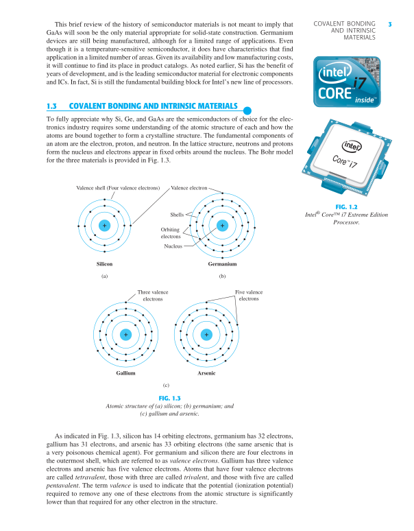
This brief review of the history of semiconductor materials is not meant to imply thatGaAs will soon be the only material appropriate for solid-state construction. Germaniumdevices are still being manufactured, although for a limited range of applications. Eventhough it is a temperature-sensitive semiconductor, it does have characteristics that findapplication in a limited number of areas. Given its availability and low manufacturing costs,it will continue to find its place in product catalogs. As noted earlier, Si has the benefit ofyears of development, and is the leading semiconductor material for electronic componentsand ICs. In fact, Si is still the fundamental building block for Intel’s new line of processors.1.3COVALENT BONDING AND INTRINSIC MATERIALS ●To fully appreciate why Si, Ge, and GaAs are the semiconductors of choice for the elec-tronics industry requires some understanding of the atomic structure of each and how theatoms are bound together to form a crystalline structure. The fundamental components ofan atom are the electron, proton, and neutron. In the lattice structure, neutrons and protonsform the nucleus and electrons appear in fixed orbits around the nucleus. The Bohr modelfor the three materials is provided in Fig. 1.3 .3COVALENT BONDINGAND INTRINSICMATERIALSFIG. 1.2Intel® Core™ i7 Extreme EditionProcessor.Three valenceelectronsGallium+Five valenceelectronsArsenic+(c)Valence electronValence shell (Four valence electrons)ShellsNucleusOrbitingelectronsSilicon+Germanium+(a)(b)FIG. 1.3Atomic structure of (a) silicon; (b) germanium; and(c) gallium and arsenic.As indicated in Fig. 1.3 , silicon has 14 orbiting electrons, germanium has 32 electrons,gallium has 31 electrons, and arsenic has 33 orbiting electrons (the same arsenic that isa very poisonous chemical agent). For germanium and silicon there are four electrons inthe outermost shell, which are referred to as valence electrons . Gallium has three valenceelectrons and arsenic has five valence electrons. Atoms that have four valence electronsare called tetravalent , those with three are called trivalent , and those with five are calledpentavalent . The term valence is used to indicate that the potential (ionization potential)required to remove any one of these electrons from the atomic structure is significantlylower than that required for any other electron in the structure.
textbook p. 3PDF p. 24
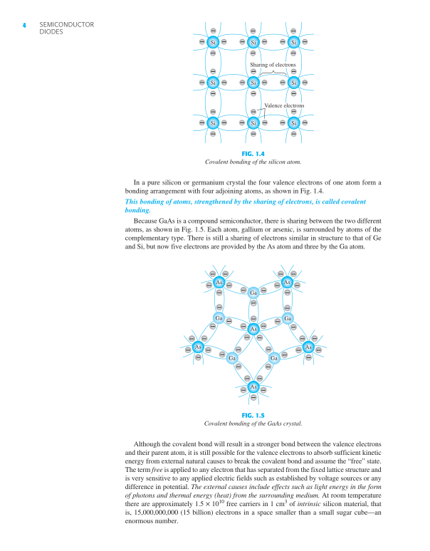
SEMICONDUCTORDIODES4In a pure silicon or germanium crystal the four valence electrons of one atom form abonding arrangement with four adjoining atoms, as shown in Fig. 1.4 .This bonding of atoms, strengthened by the sharing of electrons, is called covalentbonding.Because GaAs is a compound semiconductor, there is sharing between the two differentatoms, as shown in Fig. 1.5 . Each atom, gallium or arsenic, is surrounded by atoms of thecomplementary type. There is still a sharing of electrons similar in structure to that of Geand Si, but now five electrons are provided by the As atom and three by the Ga atom.Si–––––––––––––––––––––––––––––––––––SiSiSiSiSiSiSiSiValence electronsSharing of electrons–FIG. 1.4Covalent bonding of the silicon atom.–––––––––––––––––––––––––––––––––––––––––––AsAsAsAsAsAsGaGaGaGaGa––FIG. 1.5Covalent bonding of the GaAs crystal.Although the covalent bond will result in a stronger bond between the valence electronsand their parent atom, it is still possible for the valence electrons to absorb sufficient kineticenergy from external natural causes to break the covalent bond and assume the “free” state.The term free is applied to any electron that has separated from the fixed lattice structure andis very sensitive to any applied electric fields such as established by voltage sources or anydifference in potential. The external causes include effects such as light energy in the formof photons and thermal energy (heat) from the surrounding medium. At room temperaturethere are approximately 1.5 : 10 10 free carriers in 1 cm 3 of intrinsic silicon material, thatis, 15,000,000,000 (15 billion) electrons in a space smaller than a small sugar cube—anenormous number.
textbook p. 4PDF p. 25
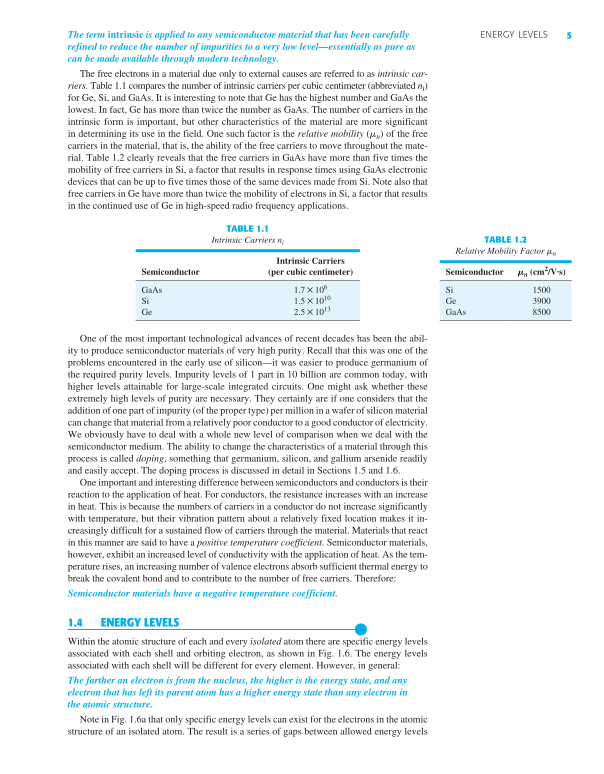
5ENERGY LEVELSThe term intrinsic is applied to any semiconductor material that has been carefullyrefined to reduce the number of impurities to a very low level—essentially as pure ascan be made available through modern technology.The free electrons in a material due only to external causes are referred to as intrinsic car-riers. Table 1.1 compares the number of intrinsic carriers per cubic centimeter (abbreviated n i )for Ge, Si, and GaAs. It is interesting to note that Ge has the highest number and GaAs thelowest. In fact, Ge has more than twice the number as GaAs. The number of carriers in theintrinsic form is important, but other characteristics of the material are more significantin determining its use in the field. One such factor is the relative mobility (m n ) of the freecarriers in the material, that is, the ability of the free carriers to move throughout the mate-rial. Table 1.2 clearly reveals that the free carriers in GaAs have more than five times themobility of free carriers in Si, a factor that results in response times using GaAs electronicdevices that can be up to five times those of the same devices made from Si. Note also thatfree carriers in Ge have more than twice the mobility of electrons in Si, a factor that resultsin the continued use of Ge in high-speed radio frequency applications.TABLE 1.1Intrinsic Carriers n iSemiconductorIntrinsic Carriers(per cubic centimeter)GaAs1.7 : 10 6Si1.5 : 10 10Ge2.5 : 10 13TABLE 1.2Relative Mobility Factor m nSemiconductorM n (cm 2 /V·s)Si1500Ge3900GaAs8500One of the most important technological advances of recent decades has been the abil-ity to produce semiconductor materials of very high purity. Recall that this was one of theproblems encountered in the early use of silicon—it was easier to produce germanium ofthe required purity levels. Impurity levels of 1 part in 10 billion are common today, withhigher levels attainable for large-scale integrated circuits. One might ask whether theseextremely high levels of purity are necessary. They certainly are if one considers that theaddition of one part of impurity (of the proper type) per million in a wafer of silicon materialcan change that material from a relatively poor conductor to a good conductor of electricity.We obviously have to deal with a whole new level of comparison when we deal with thesemiconductor medium. The ability to change the characteristics of a material through thisprocess is called doping , something that germanium, silicon, and gallium arsenide readilyand easily accept. The doping process is discussed in detail in Sections 1 . 5 and 1 . 6 .One important and interesting difference between semiconductors and conductors is theirreaction to the application of heat. For conductors, the resistance increases with an increasein heat. This is because the numbers of carriers in a conductor do not increase significantlywith temperature, but their vibration pattern about a relatively fixed location makes it in-creasingly difficult for a sustained flow of carriers through the material. Materials that reactin this manner are said to have a positive temperature coefficient. Semiconductor materials,however, exhibit an increased level of conductivity with the application of heat. As the tem-perature rises, an increasing number of valence electrons absorb sufficient thermal energy tobreak the covalent bond and to contribute to the number of free carriers. Therefore:Semiconductor materials have a negative temperature coefficient.1.4ENERGY LEVELS●Within the atomic structure of each and every isolated atom there are specific energy levelsassociated with each shell and orbiting electron, as shown in Fig. 1.6 . The energy levelsassociated with each shell will be different for every element. However, in general:The farther an electron is from the nucleus, the higher is the energy state, and anyelectron that has left its parent atom has a higher energy state than any electron inthe atomic structure.Note in Fig. 1.6a that only specific energy levels can exist for the electrons in the atomicstructure of an isolated atom. The result is a series of gaps between allowed energy levels
textbook p. 5PDF p. 26
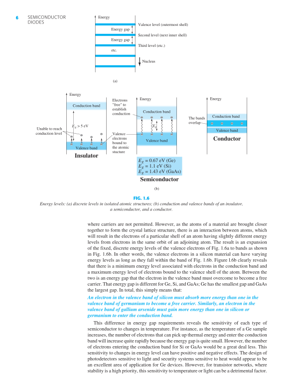
SEMICONDUCTORDIODES6where carriers are not permitted. However, as the atoms of a material are brought closertogether to form the crystal lattice structure, there is an interaction between atoms, whichwill result in the electrons of a particular shell of an atom having slightly different energylevels from electrons in the same orbit of an adjoining atom. The result is an expansionof the fixed, discrete energy levels of the valence electrons of Fig. 1.6a to bands as shownin Fig. 1.6b . In other words, the valence electrons in a silicon material can have varyingenergy levels as long as they fall within the band of Fig. 1.6b . Figure l.6b clearly revealsthat there is a minimum energy level associated with electrons in the conduction band anda maximum energy level of electrons bound to the valence shell of the atom. Between thetwo is an energy gap that the electron in the valence band must overcome to become a freecarrier. That energy gap is different for Ge, Si, and GaAs; Ge has the smallest gap and GaAsthe largest gap. In total, this simply means that:An electron in the valence band of silicon must absorb more energy than one in thevalence band of germanium to become a free carrier. Similarly, an electron in thevalence band of gallium arsenide must gain more energy than one in silicon orgermanium to enter the conduction band.This difference in energy gap requirements reveals the sensitivity of each type ofsemiconductor to changes in temperature. For instance, as the temperature of a Ge sampleincreases, the number of electrons that can pick up thermal energy and enter the conductionband will increase quite rapidly because the energy gap is quite small. However, the numberof electrons entering the conduction band for Si or GaAs would be a great deal less. Thissensitivity to changes in energy level can have positive and negative effects. The design ofphotodetectors sensitive to light and security systems sensitive to heat would appear to bean excellent area of application for Ge devices. However, for transistor networks, wherestability is a high priority, this sensitivity to temperature or light can be a detrimental factor.Energy gapEnergy gapetc.Valence level (outermost shell)Second level (next inner shell)Third level (etc.)EnergyNucleus(a)EnergyEnergyEnergyE > 5 eVgValence bandConduction bandValence bandConduction bandConduction bandThe bandsoverlapElectrons"free" toestablishconductionValenceelectronsbound tothe atomicstuctureE = 0.67 eV (Ge)gE = 1.1 eV (Si)gE = 1.43 eV (GaAs)gInsulatorSemiconductor(b)EgEValence bandConductor––––––––––––––––Unable to reachconduction level––––FIG. 1.6Energy levels: (a) discrete levels in isolated atomic structures; (b) conduction and valence bands of an insulator,a semiconductor, and a conductor.
textbook p. 6PDF p. 27
7n-TYPE AND p-TYPEMATERIALSThe energy gap also reveals which elements are useful in the construction of light-emittingdevices such as light-emitting diodes (LEDs), which will be introduced shortly. The widerthe energy gap, the greater is the possibility of energy being released in the form of visibleor invisible (infrared) light waves. For conductors, the overlapping of valence and conduc-tion bands essentially results in all the additional energy picked up by the electrons beingdissipated in the form of heat. Similarly, for Ge and Si, because the energy gap is so small,most of the electrons that pick up sufficient energy to leave the valence band end up in theconduction band, and the energy is dissipated in the form of heat. However, for GaAs thegap is sufficiently large to result in significant light radiation. For LEDs ( Section 1.9 ) thelevel of doping and the materials chosen determine the resulting color.Before we leave this subject, it is important to underscore the importance of understand-ing the units used for a quantity. In Fig. 1.6 the units of measurement are electron volts (eV).The unit of measure is appropriate because W (energy) = QV (as derived from the definingequation for voltage: V = W / Q ). Substituting the charge of one electron and a potential dif-ference of 1 V results in an energy level referred to as one electron volt .That is,W = QV= (1.6 * 10-19 C)(1 V)= 1.6 * 10-19 Jand1 eV = 1.6 * 10-19 J(1.1)1.5n -TYPE AND p -TYPE MATERIALS●Because Si is the material used most frequently as the base (substrate) material in the con-struction of solid-state electronic devices, the discussion to follow in this and the next fewsections deals solely with Si semiconductors. Because Ge, Si, and GaAs share a similarcovalent bonding, the discussion can easily be extended to include the use of the othermaterials in the manufacturing process.As indicated earlier, the characteristics of a semiconductor material can be altered sig-nificantly by the addition of specific impurity atoms to the relatively pure semiconductormaterial. These impurities, although only added at 1 part in 10 million, can alter the bandstructure sufficiently to totally change the electrical properties of the material.A semiconductor material that has been subjected to the doping process is called anextrinsic material.There are two extrinsic materials of immeasureable importance to semiconductor devicefabrication: n -type and p -type materials. Each is described in some detail in the followingsubsections.n -Type MaterialBoth n -type and p -type materials are formed by adding a predetermined number of impurityatoms to a silicon base. An n -type material is created by introducing impurity elements thathave five valence electrons ( pentavalent ), such as antimony , arsenic , and phosphorus. Each isa member of a subset group of elements in the Periodic Table of Elements referred to as GroupV because each has five valence electrons. The effect of such impurity elements is indicated inFig. 1.7 (using antimony as the impurity in a silicon base). Note that the four covalent bondsare still present. There is, however, an additional fifth electron due to the impurity atom, whichis unassociated with any particular covalent bond. This remaining electron, loosely bound toits parent (antimony) atom, is relatively free to move within the newly formed n -type material.Since the inserted impurity atom has donated a relatively “free” electron to the structure:Diffused impurities with five valence electrons are called donor atoms.It is important to realize that even though a large number of free carriers have been estab-lished in the n -type material, it is still electrically neutral since ideally the number of posi-tively charged protons in the nuclei is still equal to the number of free and orbiting negativelycharged electrons in the structure.
textbook p. 7PDF p. 28
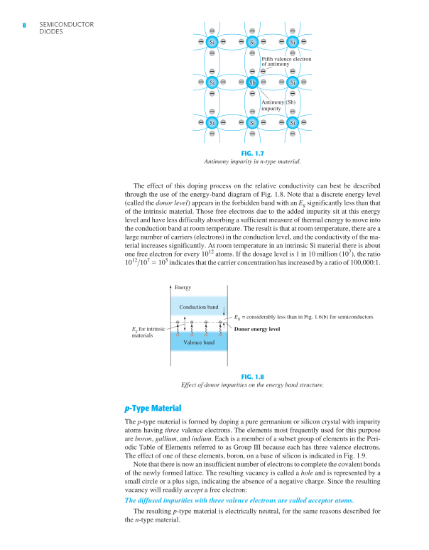
SEMICONDUCTORDIODES8The effect of this doping process on the relative conductivity can best be describedthrough the use of the energy-band diagram of Fig. 1.8 . Note that a discrete energy level(called the donor level ) appears in the forbidden band with an E g significantly less than thatof the intrinsic material. Those free electrons due to the added impurity sit at this energylevel and have less difficulty absorbing a sufficient measure of thermal energy to move intothe conduction band at room temperature. The result is that at room temperature, there are alarge number of carriers (electrons) in the conduction level, and the conductivity of the ma-terial increases significantly. At room temperature in an intrinsic Si material there is aboutone free electron for every 10 12 atoms. If the dosage level is 1 in 10 million (10 7 ), the ratio10 12 >10 7 10 5 indicates that the carrier concentration has increased by a ratio of 100,000:1.Antimony (Sb)impuritySiSiSiSiSbSiSiSiSiFifth valence electronof antimony–––––––––––––––––––––––––––––––––––––FIG. 1.7Antimony impurity in n-type material.EnergyConduction bandValence bandDonor energy levelgE = considerably less than in Fig. 1.6(b) for semiconductorsEg for intrinsicmaterials––––––––FIG. 1.8Effect of donor impurities on the energy band structure.p -Type MaterialThe p -type material is formed by doping a pure germanium or silicon crystal with impurityatoms having three valence electrons. The elements most frequently used for this purposeare boron , gallium , and indium . Each is a member of a subset group of elements in the Peri-odic Table of Elements referred to as Group III because each has three valence electrons.The effect of one of these elements, boron, on a base of silicon is indicated in Fig. 1.9 .Note that there is now an insufficient number of electrons to complete the covalent bondsof the newly formed lattice. The resulting vacancy is called a hole and is represented by asmall circle or a plus sign, indicating the absence of a negative charge. Since the resultingvacancy will readily accept a free electron:The diffused impurities with three valence electrons are called acceptor atoms.The resulting p -type material is electrically neutral, for the same reasons described forthe n -type material.
textbook p. 8PDF p. 29
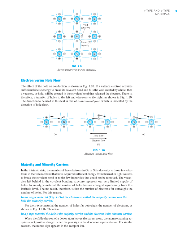
9n-TYPE AND p-TYPEMATERIALSElectron versus Hole FlowThe effect of the hole on conduction is shown in Fig. 1.10 . If a valence electron acquiressufficient kinetic energy to break its covalent bond and fills the void created by a hole, thena vacancy, or hole, will be created in the covalent bond that released the electron. There is,therefore, a transfer of holes to the left and electrons to the right, as shown in Fig. 1.10 .The direction to be used in this text is that of conventional flow , which is indicated by thedirection of hole flow.Si–––––––––––––––––––––––––––––––––––SiSiSiBSiSiSiSiBoron (B)impurityVoid(O or +)FIG. 1.9Boron impurity in p-type material.––––––––BSi––––––BSiHole flowElectron flow(a)(b)(c)–––––––BSiFIG. 1.10Electron versus hole flow.Majority and Minority CarriersIn the intrinsic state, the number of free electrons in Ge or Si is due only to those few elec-trons in the valence band that have acquired sufficient energy from thermal or light sourcesto break the covalent bond or to the few impurities that could not be removed. The vacan-cies left behind in the covalent bonding structure represent our very limited supply ofholes. In an n -type material, the number of holes has not changed significantly from thisintrinsic level. The net result, therefore, is that the number of electrons far outweighs thenumber of holes. For this reason:In an n-type material ( Fig. 1.11a ) the electron is called the majority carrier and thehole the minority carrier.For the p -type material the number of holes far outweighs the number of electrons, asshown in Fig. 1.11b . Therefore:In a p-type material the hole is the majority carrier and the electron is the minority carrier.When the fifth electron of a donor atom leaves the parent atom, the atom remaining ac-quires a net positive charge: hence the plus sign in the donor-ion representation. For similarreasons, the minus sign appears in the acceptor ion.
textbook p. 9PDF p. 30
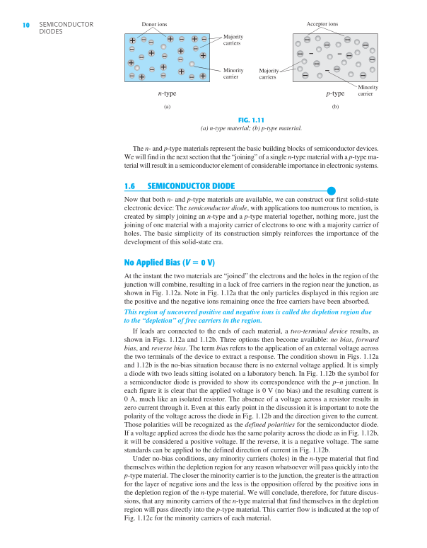
SEMICONDUCTORDIODES10The n - and p -type materials represent the basic building blocks of semiconductor devices.We will find in the next section that the “joining” of a single n -type material with a p -type ma-terial will result in a semiconductor element of considerable importance in electronic systems.1.6SEMICONDUCTOR DIODE●Now that both n - and p -type materials are available, we can construct our first solid-stateelectronic device: The semiconductor diode , with applications too numerous to mention, iscreated by simply joining an n -type and a p -type material together, nothing more, just thejoining of one material with a majority carrier of electrons to one with a majority carrier ofholes. The basic simplicity of its construction simply reinforces the importance of thedevelopment of this solid-state era.No Applied Bias ( V 0 V)At the instant the two materials are “joined” the electrons and the holes in the region of thejunction will combine, resulting in a lack of free carriers in the region near the junction, asshown in Fig. 1.12a . Note in Fig. 1.12a that the only particles displayed in this region arethe positive and the negative ions remaining once the free carriers have been absorbed.This region of uncovered positive and negative ions is called the depletion region dueto the “depletion” of free carriers in the region.If leads are connected to the ends of each material, a two-terminal device results, asshown in Figs. 1.12a and 1.12b . Three options then become available: no bias , forwardbias , and reverse bias . The term bias refers to the application of an external voltage acrossthe two terminals of the device to extract a response. The condition shown in Figs. 1.12aand 1.12b is the no-bias situation because there is no external voltage applied. It is simplya diode with two leads sitting isolated on a laboratory bench. In Fig. 1.12b the symbol fora semiconductor diode is provided to show its correspondence with the p – n junction. Ineach figure it is clear that the applied voltage is 0 V (no bias) and the resulting current is0 A, much like an isolated resistor. The absence of a voltage across a resistor results inzero current through it. Even at this early point in the discussion it is important to note thepolarity of the voltage across the diode in Fig. 1.12b and the direction given to the current.Those polarities will be recognized as the defined polarities for the semiconductor diode.If a voltage applied across the diode has the same polarity across the diode as in Fig. 1.12b ,it will be considered a positive voltage. If the reverse, it is a negative voltage. The samestandards can be applied to the defined direction of current in Fig. 1.12b .Under no-bias conditions, any minority carriers (holes) in the n -type material that findthemselves within the depletion region for any reason whatsoever will pass quickly into thep -type material. The closer the minority carrier is to the junction, the greater is the attractionfor the layer of negative ions and the less is the opposition offered by the positive ions inthe depletion region of the n -type material. We will conclude, therefore, for future discus-sions, that any minority carriers of the n -type material that find themselves in the depletionregion will pass directly into the p -type material. This carrier flow is indicated at the top ofFig. 1.12c for the minority carriers of each material.+–MinoritycarrierMinoritycarrierp-typen-typeDonor ionsMajoritycarriersAcceptor ionsMajoritycarriers++++++++++––––––––––(a)(b)––––––––––––––––FIG. 1.11(a) n-type material; (b) p-type material.
textbook p. 10PDF p. 31
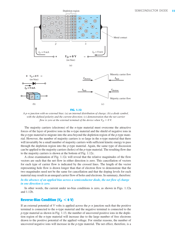
11SEMICONDUCTOR DIODEThe majority carriers (electrons) of the n -type material must overcome the attractiveforces of the layer of positive ions in the n -type material and the shield of negative ions inthe p -type material to migrate into the area beyond the depletion region of the p -type mate-rial. However, the number of majority carriers is so large in the n -type material that therewill invariably be a small number of majority carriers with sufficient kinetic energy to passthrough the depletion region into the p -type material. Again, the same type of discussioncan be applied to the majority carriers (holes) of the p -type material. The resulting flow dueto the majority carriers is shown at the bottom of Fig. 1.12c .A close examination of Fig. 1.12c will reveal that the relative magnitudes of the flowvectors are such that the net flow in either direction is zero. This cancellation of vectorsfor each type of carrier flow is indicated by the crossed lines. The length of the vectorrepresenting hole flow is drawn longer than that of electron flow to demonstrate that thetwo magnitudes need not be the same for cancellation and that the doping levels for eachmaterial may result in an unequal carrier flow of holes and electrons. In summary, therefore:In the absence of an applied bias across a semiconductor diode, the net flow of chargein one direction is zero.In other words, the current under no-bias conditions is zero, as shown in Figs. 1.12aand 1.12b .Reverse-Bias Condition ( V D * 0 V)If an external potential of V volts is applied across the p – n junction such that the positiveterminal is connected to the n -type material and the negative terminal is connected to thep -type material as shown in Fig. 1.13 , the number of uncovered positive ions in the deple-tion region of the n -type material will increase due to the large number of free electronsdrawn to the positive potential of the applied voltage. For similar reasons, the number ofuncovered negative ions will increase in the p -type material. The net effect, therefore, is appnID = 0 mAVD = 0 V(no bias)+ VD = 0 V –(no bias)ID = 0 mAnDepletion region++++++++++ ++–+++++++++++++++–––––––––––––––––––––––––––––––––––––––––(a)Minority carrier flowMajority carrier flow(b)(c)Metal contactIelectronIelectronIholeIholeID = 0 mAID = 0 mAFIG. 1.12A p–n junction with no external bias: (a) an internal distribution of charge; (b) a diode symbol,with the defined polarity and the current direction; (c) demonstration that the net carrierflow is zero at the external terminal of the device when V D 0 V.
textbook p. 11PDF p. 32
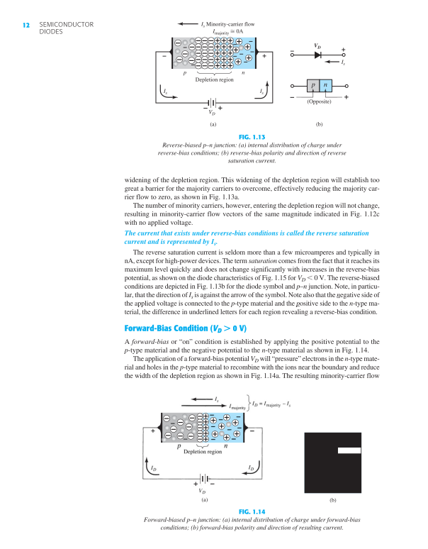
SEMICONDUCTORDIODES12widening of the depletion region. This widening of the depletion region will establish toogreat a barrier for the majority carriers to overcome, effectively reducing the majority car-rier flow to zero, as shown in Fig. 1.13a .The number of minority carriers, however, entering the depletion region will not change,resulting in minority-carrier flow vectors of the same magnitude indicated in Fig. 1.12cwith no applied voltage.The current that exists under reverse-bias conditions is called the reverse saturationcurrent and is represented by I s .The reverse saturation current is seldom more than a few microamperes and typically innA, except for high-power devices. The term saturation comes from the fact that it reaches itsmaximum level quickly and does not change significantly with increases in the reverse-biaspotential, as shown on the diode characteristics of Fig. 1.15 for V D 0 V. The reverse-biasedconditions are depicted in Fig. 1.13b for the diode symbol and p – n junction. Note, in particu-lar, that the direction of I s is against the arrow of the symbol. Note also that the n egative side ofthe applied voltage is connected to the p -type material and the p ositive side to the n -type ma-terial, the difference in underlined letters for each region revealing a reverse-bias condition.Forward-Bias Condition ( V D + 0 V)A forward-bias or “on” condition is established by applying the positive potential to thep -type material and the negative potential to the n -type material as shown in Fig. 1.14 .The application of a forward-bias potential V D will “pressure” electrons in the n -type mate-rial and holes in the p -type material to recombine with the ions near the boundary and reducethe width of the depletion region as shown in Fig. 1.14a . The resulting minority-carrier flowpnIsVD+–pnDepletion region++++++++++++ + +++ +++++––––––––––––––––––– ––––––––––Is Minority-carrier flowImajority 0AIsIs(Opposite)+–(b)VD +–(a)FIG. 1.13Reverse-biased p–n junction: (a) internal distribution of charge underreverse-bias conditions; (b) reverse-bias polarity and direction of reversesaturation current.(a)+–––––– –––++ ++++++++++–––––FIG. 1.14Forward-biased p–n junction: (a) internal distribution of charge under forward-biasconditions; (b) forward-bias polarity and direction of resulting current.(b)
textbook p. 12PDF p. 33
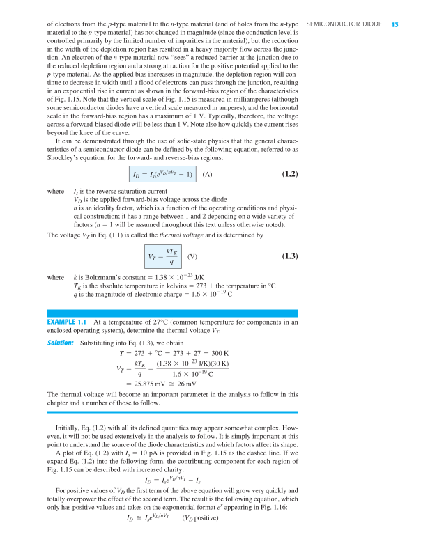
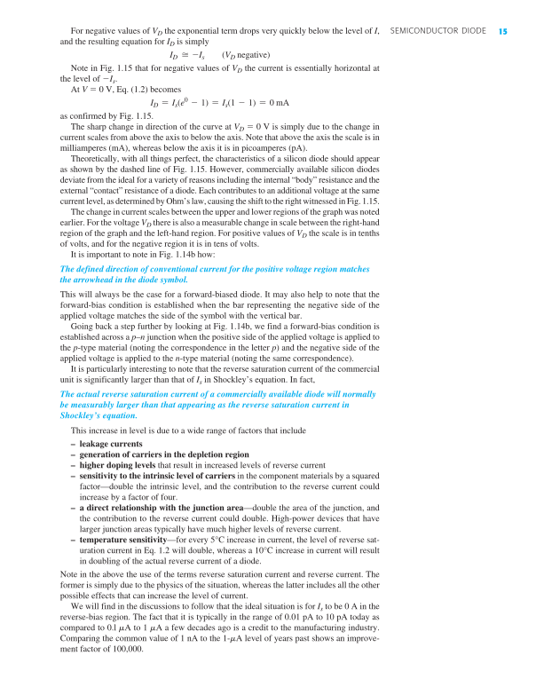
13SEMICONDUCTOR DIODEof electrons from the p -type material to the n -type material (and of holes from the n -typematerial to the p -type material) has not changed in magnitude (since the conduction level iscontrolled primarily by the limited number of impurities in the material), but the reductionin the width of the depletion region has resulted in a heavy majority flow across the junc-tion. An electron of the n -type material now “sees” a reduced barrier at the junction due tothe reduced depletion region and a strong attraction for the positive potential applied to thep -type material. As the applied bias increases in magnitude, the depletion region will con-tinue to decrease in width until a flood of electrons can pass through the junction, resultingin an exponential rise in current as shown in the forward-bias region of the characteristicsof Fig. 1.15 . Note that the vertical scale of Fig. 1.15 is measured in milliamperes (althoughsome semiconductor diodes have a vertical scale measured in amperes), and the horizontalscale in the forward-bias region has a maximum of 1 V. Typically, therefore, the voltageacross a forward-biased diode will be less than 1 V. Note also how quickly the current risesbeyond the knee of the curve.It can be demonstrated through the use of solid-state physics that the general charac-teristics of a semiconductor diode can be defined by the following equation, referred to asShockley’s equation, for the forward- and reverse-bias regions:ID = Is(eVD>nVT - 1) (A)(1.2)whereI s is the reverse saturation currentV D is the applied forward-bias voltage across the dioden is an ideality factor, which is a function of the operating conditions and physi-cal construction; it has a range between 1 and 2 depending on a wide variety offactors ( n 1 will be assumed throughout this text unless otherwise noted).The voltage V T in Eq. (1.1) is called the thermal voltage and is determined byVT = kTKq (V)(1.3)wherek is Boltzmann’s constant 1.38 10 23 J/KT K is the absolute temperature in kelvins 273 the temperature in °Cq is the magnitude of electronic charge 1.6 10 19 CEXAMPLE 1.1 At a temperature of 27°C (common temperature for components in anenclosed operating system), determine the thermal voltage V T .Solution: Substituting into Eq. (1.3), we obtainT = 273 + C = 273 + 27 = 300 KVT = kTKq= (1.38 * 10-23 J/K)(30 K)1.6 * 10-19 C= 25.875 mV 26 mVThe thermal voltage will become an important parameter in the analysis to follow in thischapter and a number of those to follow.Initially, Eq. (1.2) with all its defined quantities may appear somewhat complex. How-ever, it will not be used extensively in the analysis to follow. It is simply important at thispoint to understand the source of the diode characteristics and which factors affect its shape.A plot of Eq. (1.2) with I s 10 pA is provided in Fig. 1.15 as the dashed line. If weexpand Eq. (1.2) into the following form, the contributing component for each region ofFig. 1.15 can be described with increased clarity:ID = IseVD>nVT - IsFor positive values of V D the first term of the above equation will grow very quickly andtotally overpower the effect of the second term. The result is the following equation, whichonly has positive values and takes on the exponential format e x appearing in Fig. 1.16 :ID IseVD>nVT (VD positive)
textbook p. 13PDF p. 34
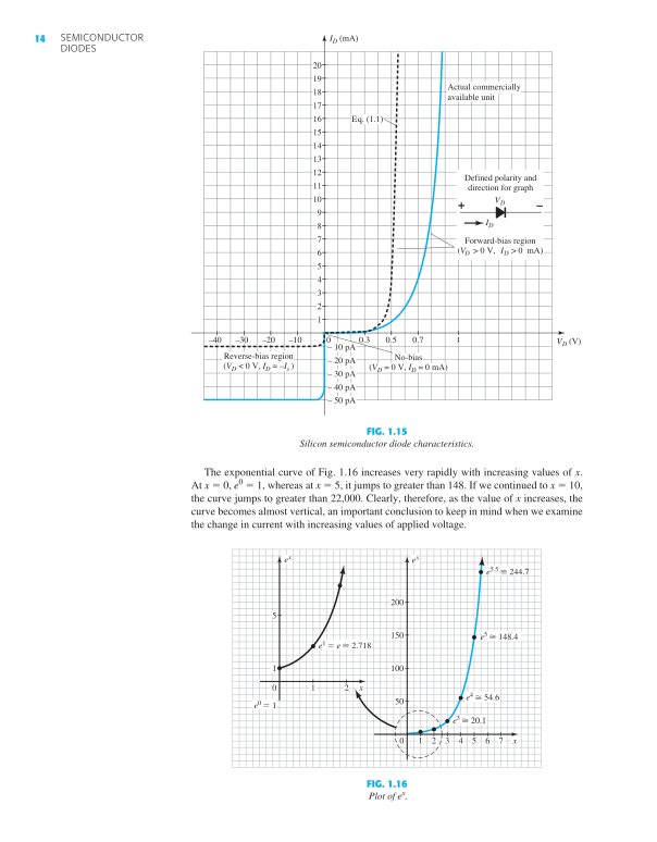
SEMICONDUCTORDIODES14The exponential curve of Fig. 1.16 increases very rapidly with increasing values of x .At x 0, e 0 1, whereas at x 5, it jumps to greater than 148. If we continued to x 10,the curve jumps to greater than 22,000. Clearly, therefore, as the value of x increases, thecurve becomes almost vertical, an important conclusion to keep in mind when we examinethe change in current with increasing values of applied voltage.10111213141516171819201234567890.30.50.71–10–20–30–40ID (mA)(V)DVDV–+Defined polarity anddirection for graphForward-bias region(V > 0 V, I > 0 mA)DIDVID– 20 pA– 30 pA– 40 pA– 50 pA0No-bias(VD = 0 V, ID = 0 mA)– 10 pAReverse-bias region(VD < 0 V, ID = –Is )Eq. (1.1)Actual commerciallyavailable unitFIG. 1.15Silicon semiconductor diode characteristics.234567xx10e3 20.1e4 54.6e5 148.4e5.5 244.750200150100e1 e 2.718exex1215e0 10FIG. 1.16Plot of e x .
textbook p. 14PDF p. 35
15SEMICONDUCTOR DIODEFor negative values of V D the exponential term drops very quickly below the level of I ,and the resulting equation for I D is simplyID -Is (VD negative)Note in Fig. 1.15 that for negative values of V D the current is essentially horizontal atthe level of I s .At V 0 V, Eq. (1.2) becomesID = Is(e0 - 1) = Is(1 - 1) = 0 mAas confirmed by Fig. 1.15 .The sharp change in direction of the curve at V D 0 V is simply due to the change incurrent scales from above the axis to below the axis. Note that above the axis the scale is inmilliamperes (mA), whereas below the axis it is in picoamperes (pA).Theoretically, with all things perfect, the characteristics of a silicon diode should appearas shown by the dashed line of Fig. 1.15 . However, commercially available silicon diodesdeviate from the ideal for a variety of reasons including the internal “body” resistance and theexternal “contact” resistance of a diode. Each contributes to an additional voltage at the samecurrent level, as determined by Ohm’s law, causing the shift to the right witnessed in Fig. 1.15 .The change in current scales between the upper and lower regions of the graph was notedearlier. For the voltage V D there is also a measurable change in scale between the right-handregion of the graph and the left-hand region. For positive values of V D the scale is in tenthsof volts, and for the negative region it is in tens of volts.It is important to note in Fig. 1.14b how:The defined direction of conventional current for the positive voltage region matchesthe arrowhead in the diode symbol.This will always be the case for a forward-biased diode. It may also help to note that theforward-bias condition is established when the bar representing the negative side of theapplied voltage matches the side of the symbol with the vertical bar.Going back a step further by looking at Fig. 1.14b , we find a forward-bias condition isestablished across a p – n junction when the positive side of the applied voltage is applied tothe p -type material (noting the correspondence in the letter p ) and the negative side of theapplied voltage is applied to the n -type material (noting the same correspondence).It is particularly interesting to note that the reverse saturation current of the commercialunit is significantly larger than that of I s in Shockley’s equation. In fact,The actual reverse saturation current of a commercially available diode will normallybe measurably larger than that appearing as the reverse saturation current inShockley’s equation.This increase in level is due to a wide range of factors that include– leakage currents– generation of carriers in the depletion region– higher doping levels that result in increased levels of reverse current– sensitivity to the intrinsic level of carriers in the component materials by a squaredfactor—double the intrinsic level, and the contribution to the reverse current couldincrease by a factor of four.– a direct relationship with the junction area—double the area of the junction, andthe contribution to the reverse current could double. High-power devices that havelarger junction areas typically have much higher levels of reverse current.– temperature sensitivity—for every 5°C increase in current, the level of reverse sat-uration current in Eq. 1.2 will double, whereas a 10°C increase in current will resultin doubling of the actual reverse current of a diode.Note in the above the use of the terms reverse saturation current and reverse current. Theformer is simply due to the physics of the situation, whereas the latter includes all the otherpossible effects that can increase the level of current.We will find in the discussions to follow that the ideal situation is for I s to be 0 A in thereverse-bias region. The fact that it is typically in the range of 0.01 pA to 10 pA today ascompared to 0.l mA to 1 mA a few decades ago is a credit to the manufacturing industry.Comparing the common value of 1 nA to the 1-mA level of years past shows an improve-ment factor of 100,000.
textbook p. 15PDF p. 36
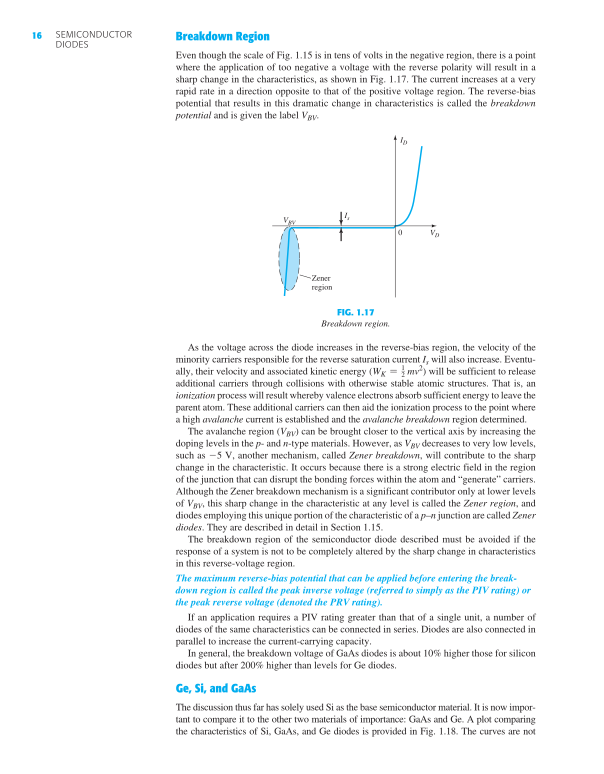
SEMICONDUCTORDIODES16Breakdown RegionEven though the scale of Fig. 1.15 is in tens of volts in the negative region, there is a pointwhere the application of too negative a voltage with the reverse polarity will result in asharp change in the characteristics, as shown in Fig. 1.17 . The current increases at a veryrapid rate in a direction opposite to that of the positive voltage region. The reverse-biaspotential that results in this dramatic change in characteristics is called the breakdownpotential and is given the label V BV .IDIsVDVBV0ZenerregionFIG. 1.17Breakdown region.As the voltage across the diode increases in the reverse-bias region, the velocity of theminority carriers responsible for the reverse saturation current I s will also increase. Eventu-ally, their velocity and associated kinetic energy (WK = 12 mv2) will be sufficient to releaseadditional carriers through collisions with otherwise stable atomic structures. That is, anionization process will result whereby valence electrons absorb sufficient energy to leave theparent atom. These additional carriers can then aid the ionization process to the point wherea high avalanche current is established and the avalanche breakdown region determined.The avalanche region ( V BV ) can be brought closer to the vertical axis by increasing thedoping levels in the p - and n -type materials. However, as V BV decreases to very low levels,such as 5 V, another mechanism, called Zener breakdown , will contribute to the sharpchange in the characteristic. It occurs because there is a strong electric field in the regionof the junction that can disrupt the bonding forces within the atom and “generate” carriers.Although the Zener breakdown mechanism is a significant contributor only at lower levelsof V BV , this sharp change in the characteristic at any level is called the Zener region , anddiodes employing this unique portion of the characteristic of a p – n junction are called Zenerdiodes . They are described in detail in Section 1.15 .The breakdown region of the semiconductor diode described must be avoided if theresponse of a system is not to be completely altered by the sharp change in characteristicsin this reverse-voltage region.The maximum reverse-bias potential that can be applied before entering the break-down region is called the peak inverse voltage (referred to simply as the PIV rating) orthe peak reverse voltage (denoted the PRV rating).If an application requires a PIV rating greater than that of a single unit, a number ofdiodes of the same characteristics can be connected in series. Diodes are also connected inparallel to increase the current-carrying capacity.In general, the breakdown voltage of GaAs diodes is about 10% higher those for silicondiodes but after 200% higher than levels for Ge diodes.Ge, Si, and GaAsThe discussion thus far has solely used Si as the base semiconductor material. It is now impor-tant to compare it to the other two materials of importance: GaAs and Ge. A plot comparingthe characteristics of Si, GaAs, and Ge diodes is provided in Fig. 1.18 . The curves are not
textbook p. 16PDF p. 37
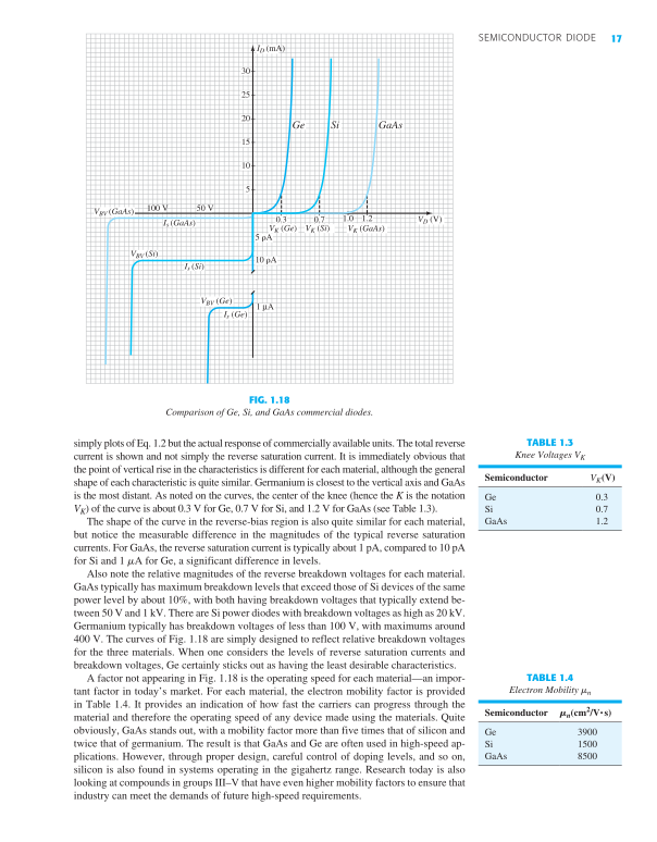
17SEMICONDUCTOR DIODEsimply plots of Eq. 1.2 but the actual response of commercially available units. The total reversecurrent is shown and not simply the reverse saturation current. It is immediately obvious thatthe point of vertical rise in the characteristics is different for each material, although the generalshape of each characteristic is quite similar. Germanium is closest to the vertical axis and GaAsis the most distant. As noted on the curves, the center of the knee (hence the K is the notationV K ) of the curve is about 0.3 V for Ge, 0.7 V for Si, and 1.2 V for GaAs (see Table 1.3 ).The shape of the curve in the reverse-bias region is also quite similar for each material,but notice the measurable difference in the magnitudes of the typical reverse saturationcurrents. For GaAs, the reverse saturation current is typically about 1 pA, compared to 10 pAfor Si and 1 mA for Ge, a significant difference in levels.Also note the relative magnitudes of the reverse breakdown voltages for each material.GaAs typically has maximum breakdown levels that exceed those of Si devices of the samepower level by about 10%, with both having breakdown voltages that typically extend be-tween 50 V and 1 kV. There are Si power diodes with breakdown voltages as high as 20 kV.Germanium typically has breakdown voltages of less than 100 V, with maximums around400 V. The curves of Fig. 1.18 are simply designed to reflect relative breakdown voltagesfor the three materials. When one considers the levels of reverse saturation currents andbreakdown voltages, Ge certainly sticks out as having the least desirable characteristics.A factor not appearing in Fig. 1.18 is the operating speed for each material—an impor-tant factor in today’s market. For each material, the electron mobility factor is providedin Table 1.4 . It provides an indication of how fast the carriers can progress through thematerial and therefore the operating speed of any device made using the materials. Quiteobviously, GaAs stands out, with a mobility factor more than five times that of silicon andtwice that of germanium. The result is that GaAs and Ge are often used in high-speed ap-plications. However, through proper design, careful control of doping levels, and so on,silicon is also found in systems operating in the gigahertz range. Research today is alsolooking at compounds in groups III–V that have even higher mobility factors to ensure thatindustry can meet the demands of future high-speed requirements.TABLE 1.3Knee Voltages V KSemiconductorV K (V)Ge0.3Si0.7GaAs1.2302520151055 A50 V100 VID (mA)1 μAVBV (Si)VBV (Ge)Is (Ge)VBV (GaAs)Is (GaAs)Is (Si)GeSiGaAs0.30.71.21.0VD (V)VK (GaAs)VK (Ge)VK (Si)10 AFIG. 1.18Comparison of Ge, Si, and GaAs commercial diodes.TABLE 1.4Electron Mobility m nSemiconductorM n (cm 2 /V~s)Ge3900Si1500GaAs8500
textbook p. 17PDF p. 38
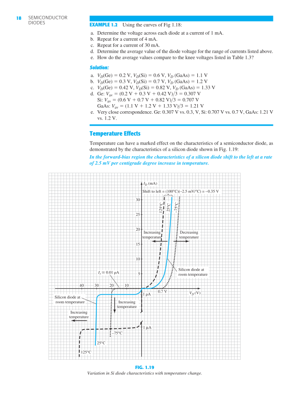
SEMICONDUCTORDIODES18EXAMPLE 1.2 Using the curves of Fig 1.18:a. Determine the voltage across each diode at a current of 1 mA.b. Repeat for a current of 4 mA.c. Repeat for a current of 30 mA.d. Determine the average value of the diode voltage for the range of currents listed above.e. How do the average values compare to the knee voltages listed in Table 1.3 ?Solution:a. V D (Ge) 0.2 V, V D (Si) 0.6 V, V D (GaAs) 1.1 Vb. V D (Ge) 0.3 V, V D (Si) 0.7 V, V D (GaAs) 1.2 Vc. V D (Ge) 0.42 V, V D (Si) 0.82 V, V D (GaAs) 1.33 Vd. Ge: V av (0.2 V 0.3 V 0.42 V)>3 0.307 VSi: V av (0.6 V 0.7 V 0.82 V)>3 0.707 VGaAs: V av (1.1 V 1.2 V 1.33 V)>3 1.21 Ve. Very close correspondence. Ge: 0.307 V vs. 0.3, V, Si: 0.707 V vs. 0.7 V, GaAs: 1.21 Vvs. 1.2 V.Temperature EffectsTemperature can have a marked effect on the characteristics of a semiconductor diode, asdemonstrated by the characteristics of a silicon diode shown in Fig. 1.19 :In the forward-bias region the characteristics of a silicon diode shift to the left at a rateof 2.5 mV per centigrade degree increase in temperature.ID (mA)Is 0.01 AShift to left = (100°C)(–2.5 mV/°C) = –0.35 VDecreasingtemperatureSilicon diode atroom temperatureSilicon diode atroom temperatureIncreasingtemperatureIncreasingtemperatureIncreasingtemperature1 A–75°C25°C125°C1 μAVD (V)0.7 V3025510152010203040125°C25°C–75°CFIG. 1.19Variation in Si diode characteristics with temperature change.
textbook p. 18PDF p. 39
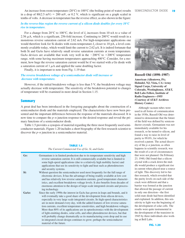
19SEMICONDUCTOR DIODEAn increase from room temperature (20°C) to 100°C (the boiling point of water) resultsin a drop of 80(2.5 mV) 200 mV, or 0.2 V, which is significant on a graph scaled intenths of volts. A decrease in temperature has the reverse effect, as also shown in the figure:In the reverse-bias region the reverse current of a silicon diode doubles for every 10°Crise in temperature.For a change from 20°C to 100°C, the level of I s increases from 10 nA to a value of2.56 mA, which is a significant, 256-fold increase. Continuing to 200°C would result in amonstrous reverse saturation current of 2.62 mA. For high-temperature applications onewould therefore look for Si diodes with room-temperature I s closer to 10 pA, a level com-monly available today, which would limit the current to 2.62 μA. It is indeed fortunate thatboth Si and GaAs have relatively small reverse saturation currents at room temperature.GaAs devices are available that work very well in the 200°C to 200°C temperaturerange, with some having maximum temperatures approaching 400°C. Consider, for a mo-ment, how huge the reverse saturation current would be if we started with a Ge diode witha saturation current of 1 mA and applied the same doubling factor.Finally, it is important to note from Fig. 1.19 that:The reverse breakdown voltage of a semiconductor diode will increase ordecrease with temperature.However, if the initial breakdown voltage is less than 5 V, the breakdown voltage mayactually decrease with temperature. The sensitivity of the breakdown potential to changesof temperature will be examined in more detail in Section 1.15 .SummaryA great deal has been introduced in the foregoing paragraphs about the construction of asemiconductor diode and the materials employed. The characteristics have now been pre-sented and the important differences between the response of the materials discussed. It isnow time to compare the p – n junction response to the desired response and reveal the pri-mary functions of a semiconductor diode.Table 1.5 provides a synopsis of material regarding the three most frequently used semi-conductor materials. Figure 1.20 includes a short biography of the first research scientist todiscover the p – n junction in a semiconductor material.FIG. 1.20Russell Ohl (1898–1987)American (Allentown, PA;Holmdel, NJ; Vista, CA) ArmySignal Corps, University ofColorado, Westinghouse, AT&T,Bell Labs Fellow, Institute ofRadio Engineers—1955(Courtesy of AT&T ArchivesHistory Center.)Although vacuum tubes wereused in all forms of communicationin the 1930s, Russell Ohl was deter-mined to demonstrate that the futureof the field was defined by semicon-ductor crystals. Germanium was notimmediately available for hisresearch, so he turned to silicon, andfound a way to raise its level ofpurity to 99.8%, for which hereceived a patent. The actual discov-ery of the p–n junction, as oftenhappens in scientific research, wasthe result of a set of circumstancesthat were not planned. On February23, 1940, Ohl found that a siliconcrystal with a crack down the mid-dle would produce a significant risein current when placed near a sourceof light. This discovery led to fur-ther research, which revealed thatthe purity levels on each side of thecrack were different and that abarrier was formed at the junctionthat allowed the passage of currentin only one direction—the firstsolid-state diode had been identifiedand explained. In addition, this sen-sitivity to light was the beginning ofthe development of solar cells. Theresults were quite instrumental inthe development of the transistor in1945 by three individuals also work-ing at Bell Labs.TABLE 1.5The Current Commercial Use of Ge, Si, and GaAsGe:Germanium is in limited production due to its temperature sensitivity and highreverse saturation current. It is still commercially available but is limited tosome high-speed applications (due to a relatively high mobility factor) andapplications that use its sensitivity to light and heat such as photodetectorsand security systems.Si:Without question the semiconductor used most frequently for the full range ofelectronic devices. It has the advantage of being readily available at low costand has relatively low reverse saturation currents, good temperature character-istics, and excellent breakdown voltage levels. It also benefits from decades ofenormous attention to the design of large-scale integrated circuits and process-ing technology.GaAs:Since the early 1990s the interest in GaAs has grown in leaps and bounds, and itwill eventually take a good share of the development from silicon devices,especially in very large scale integrated circuits. Its high-speed characteristicsare in more demand every day, with the added features of low reverse satura-tion currents, excellent temperature sensitivities, and high breakdown voltages.More than 80% of its applications are in optoelectronics with the developmentof light-emitting diodes, solar cells, and other photodetector devices, but thatwill probably change dramatically as its manufacturing costs drop and its usein integrated circuit design continues to grow; perhaps the semiconductormaterial of the future.
textbook p. 19PDF p. 40
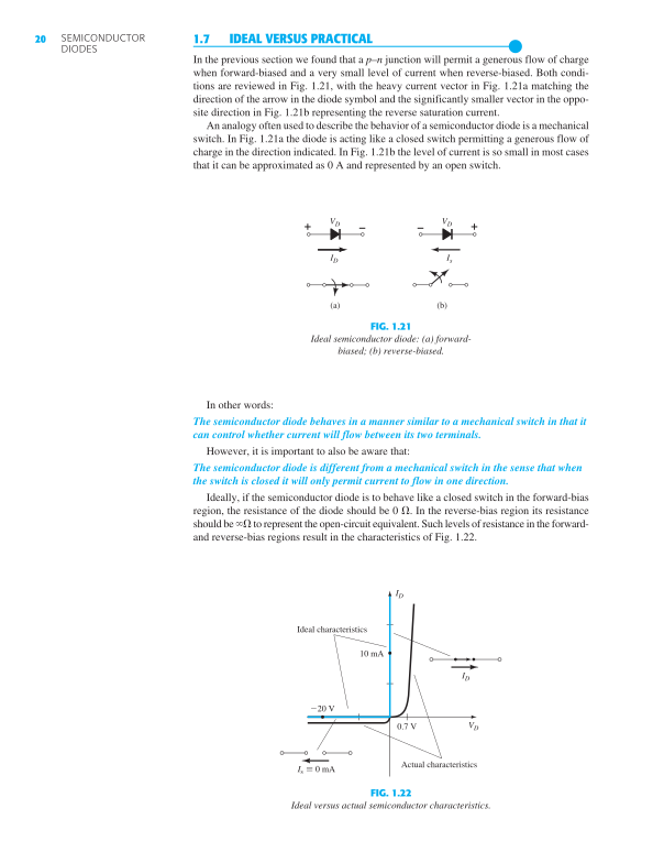
SEMICONDUCTORDIODES201.7IDEAL VERSUS PRACTICAL●In the previous section we found that a p – n junction will permit a generous flow of chargewhen forward-biased and a very small level of current when reverse-biased. Both condi-tions are reviewed in Fig. 1.21 , with the heavy current vector in Fig. 1.21a matching thedirection of the arrow in the diode symbol and the significantly smaller vector in the oppo-site direction in Fig. 1.21b representing the reverse saturation current.An analogy often used to describe the behavior of a semiconductor diode is a mechanicalswitch. In Fig. 1.21a the diode is acting like a closed switch permitting a generous flow ofcharge in the direction indicated. In Fig. 1.21b the level of current is so small in most casesthat it can be approximated as 0 A and represented by an open switch.–+VD–+VDIDIs(a)(b)FIG. 1.21Ideal semiconductor diode: (a) forward-biased; (b) reverse-biased.In other words:The semiconductor diode behaves in a manner similar to a mechanical switch in that itcan control whether current will flow between its two terminals.However, it is important to also be aware that:The semiconductor diode is different from a mechanical switch in the sense that whenthe switch is closed it will only permit current to flow in one direction.Ideally, if the semiconductor diode is to behave like a closed switch in the forward-biasregion, the resistance of the diode should be 0 . In the reverse-bias region its resistanceshould be to represent the open-circuit equivalent. Such levels of resistance in the forward-and reverse-bias regions result in the characteristics of Fig. 1.22 .Ideal characteristicsActual characteristicsIDIDVD0.7 V20 V10 mAIs 0 mAFIG. 1.22Ideal versus actual semiconductor characteristics.
textbook p. 20PDF p. 41
21RESISTANCE LEVELSThe characteristics have been superimposed to compare the ideal Si diode to a real-worldSi diode. First impressions might suggest that the commercial unit is a poor impression ofthe ideal switch. However, when one considers that the only major difference is that thecommercial diode rises at a level of 0.7 V rather than 0 V, there are a number of similaritiesbetween the two plots.When a switch is closed the resistance between the contacts is assumed to be 0 . Atthe plot point chosen on the vertical axis the diode current is 5 mA and the voltage acrossthe diode is 0 V. Substituting into Ohm’s law results inRF = VDID=0 V5 mA = 0 (short@circuit equivalent)In fact:At any current level on the vertical line, the voltage across the ideal diode is 0 V andthe resistance is 0 .For the horizontal section, if we again apply Ohm’s law, we findRR = VDID= 20 V0 mA (open@circuit equivalent)Again:Because the current is 0 mA anywhere on the horizontal line, the resistance isconsidered to be infinite ohms (an open-circuit) at any point on the axis.Due to the shape and the location of the curve for the commercial unit in the forward-biasregion there will be a resistance associated with the diode that is greater than 0 . However,if that resistance is small enough compared to other resistors of the network in series withthe diode, it is often a good approximation to simply assume the resistance of the com-mercial unit is 0 . In the reverse-bias region, if we assume the reverse saturation currentis so small it can be approximated as 0 mA, we have the same open-circuit equivalenceprovided by the open switch.The result, therefore, is that there are sufficient similarities between the ideal switch andthe semiconductor diode to make it an effective electronic device. In the next section thevarious resistance levels of importance are determined for use in the next chapter, wherethe response of diodes in an actual network is examined.1.8RESISTANCE LEVELS●As the operating point of a diode moves from one region to another the resistance of thediode will also change due to the nonlinear shape of the characteristic curve. It will be dem-onstrated in the next few paragraphs that the type of applied voltage or signal will define theresistance level of interest. Three different levels will be introduced in this section, whichwill appear again as we examine other devices. It is therefore paramount that their determi-nation be clearly understood.DC or Static ResistanceThe application of a dc voltage to a circuit containing a semiconductor diode will result inan operating point on the characteristic curve that will not change with time. The resistanceof the diode at the operating point can be found simply by finding the corresponding levelsof V D and I D as shown in Fig. 1.23 and applying the following equation:RD = VDID(1.4)The dc resistance levels at the knee and below will be greater than the resistance levelsobtained for the vertical rise section of the characteristics. The resistance levels in thereverse-bias region will naturally be quite high. Since ohmmeters typically employ a rela-tively constant-current source, the resistance determined will be at a preset current level(typically, a few milliamperes).
textbook p. 21PDF p. 42
SEMICONDUCTORDIODES22In general, therefore, the higher the current through a diode, the lower is the dc resis-tance level.Typically, the dc resistance of a diode in the active (most utilized) will range from about10 to 80 .EXAMPLE 1.3 Determine the dc resistance levels for the diode of Fig. 1.24 ata. I D 2 mA (low level)b. I D 20 mA (high level)c. V D 10 V (reverse-biased)FIG. 1.23Determining the dc resistance of a diode at aparticular operating point.FIG. 1.24Example 1.3 .Solution:a. At I D 2 mA, V D 0.5 V (from the curve) andRD = VDID= 0.5 V2 mA = 250b. At I D 20 mA, V D 0.8 V (from the curve) andRD = VDID= 0.8 V20 mA = 40
textbook p. 22PDF p. 43
23RESISTANCE LEVELSc. At V D 10 V, I D I s 1 mA (from the curve) andRD = VDID= 10 V1 mA = 10 Mclearly supporting some of the earlier comments regarding the dc resistance levels of adiode.AC or Dynamic ResistanceEq. (1.4) and Example 1.3 reveal thatthe dc resistance of a diode is independent of the shape of the characteristic in theregion surrounding the point of interest.If a sinusoidal rather than a dc input is applied, the situation will change completely. Thevarying input will move the instantaneous operating point up and down a region of the char-acteristics and thus defines a specific change in current and voltage as shown in Fig. 1.25 .With no applied varying signal, the point of operation would be the Q -point appearing onFig. 1.25 , determined by the applied dc levels. The designation Q-point is derived from theword quiescent , which means “still or unvarying.”FIG. 1.25Defining the dynamic or ac resistance.FIG. 1.26Determining the ac resistance at aQ-point.A straight line drawn tangent to the curve through the Q -point as shown in Fig. 1.26will define a particular change in voltage and current that can be used to determine the acor dynamic resistance for this region of the diode characteristics. An effort should be madeto keep the change in voltage and current as small as possible and equidistant to either sideof the Q -point. In equation form,rd = VdId(1.5)where signifies a finite change in the quantity.The steeper the slope, the lower is the value of V d for the same change in I d and thelower is the resistance. The ac resistance in the vertical-rise region of the characteristic istherefore quite small, whereas the ac resistance is much higher at low current levels.In general, therefore, the lower the Q-point of operation (smaller current or lowervoltage), the higher is the ac resistance.
textbook p. 23PDF p. 44
SEMICONDUCTORDIODES24EXAMPLE 1.4 For the characteristics of Fig. 1.27 :a. Determine the ac resistance at I D 2 mA.b. Determine the ac resistance at I D 25 mA.c. Compare the results of parts (a) and (b) to the dc resistances at each current level.V (V)DI (mA)DI051015202530240.10.30.50.70.910.80.60.40.2Δ dIΔ dIΔ dVΔ dVFIG. 1.27Example 1.4 .Solution:a. For I D 2 mA, the tangent line at I D 2 mA was drawn as shown in Fig. 1.27 and aswing of 2 mA above and below the specified diode current was chosen. At I D 4 mA,V D 0.76 V, and at I D 0 mA, V D 0.65 V. The resulting changes in current andvoltage are, respectively,Id = 4 mA - 0 mA = 4 mAandVd = 0.76 V - 0.65 V = 0.11 Vand the ac resistance isrd = VdId= 0.11 V4 mA = 27.5b. For I D 25 mA, the tangent line at I D 25 mA was drawn as shown in Fig. 1.27 anda swing of 5 mA above and below the specified diode current was chosen. At I D 30 mA,V D 0.8 V, and at I D 20 mA, V D 0.78 V. The resulting changes in current andvoltage are, respectively,Id = 30 mA - 20 mA = 10 mAandVd = 0.8 V - 0.78 V = 0.02 Vand the ac resistance isrd = VdId= 0.02 V10 mA = 2c. For I D 2 mA, V D 0.7 V andRD = VDID= 0.7 V2 mA = 350which far exceeds the r d of 27.5 .
textbook p. 24PDF p. 45
25RESISTANCE LEVELSFor I D 25 mA, V D 0.79 V andRD = VDID= 0.79 V25 mA = 31.62which far exceeds the r d of 2 .We have found the dynamic resistance graphically, but there is a basic definition in dif-ferential calculus that states:The derivative of a function at a point is equal to the slope of the tangent line drawnat that point.Equation (1.5), as defined by Fig. 1.26 , is, therefore, essentially finding the derivative ofthe function at the Q -point of operation. If we find the derivative of the general equation(1.2) for the semiconductor diode with respect to the applied forward bias and then invertthe result, we will have an equation for the dynamic or ac resistance in that region. That is,taking the derivative of Eq. (1.2) with respect to the applied bias will result inddVD(ID) =ddVD3Is(eVD>nVT - 1)4anddIDdVD =1nVT(ID + Is)after we apply differential calculus. In general, ID W Is in the vertical-slope section ofthe characteristics anddIDdVDIDnVTFlipping the result to define a resistance ratio ( R V / I ) givesdVDdID= rd = nVTIDSubstituting n 1 and VT 26 mV from Example 1.1 results inrd = 26 mVID(1.6)The significance of Eq. (1.6) must be clearly understood. It implies thatthe dynamic resistance can be found simply by substituting the quiescent value of thediode current into the equation.There is no need to have the characteristics available or to worry about sketching tangentlines as defined by Eq. (1.5). It is important to keep in mind, however, that Eq. (1.6) isaccurate only for values of I D in the vertical-rise section of the curve. For lesser values ofI D , n 2 (silicon) and the value of r d obtained must be multiplied by a factor of 2. Forsmall values of I D below the knee of the curve, Eq. (1.6) becomes inappropriate.All the resistance levels determined thus far have been defined by the p – n junction anddo not include the resistance of the semiconductor material itself (called body resistance)and the resistance introduced by the connection between the semiconductor material and theexternal metallic conductor (called contact resistance). These additional resistance levelscan be included in Eq. (1.6) by adding a resistance denoted r B :r d = 26 mVID+ rB ohms(1.7)The resistance r d , therefore, includes the dynamic resistance defined by Eq. (1.6) andthe resistance r B just introduced. The factor r B can range from typically 0.1 for high-power devices to 2 for some low-power, general-purpose diodes. For Example 1.4 the acresistance at 25 mA was calculated to be 2 . Using Eq. (1.6), we haverd = 26 mVID= 26 mV25 mA = 1.04
textbook p. 25PDF p. 46
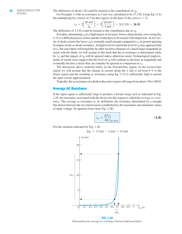
SEMICONDUCTORDIODES26The difference of about 1 could be treated as the contribution of r B .For Example 1.4 the ac resistance at 2 mA was calculated to be 27.5 . Using Eq. (1.6)but multiplying by a factor of 2 for this region (in the knee of the curve n 2),rd = 2a 26 mVIDb = 2a 26 mV2 mA b = 2(13 ) = 26The difference of 1.5 could be treated as the contribution due to r B .In reality, determining r d to a high degree of accuracy from a characteristic curve using Eq.(1.5) is a difficult process at best and the results have to be treated with skepticism. At low lev-els of diode current the factor r B is normally small enough compared to r d to permit ignoringits impact on the ac diode resistance. At high levels of current the level of r B may approach thatof r d , but since there will frequently be other resistive elements of a much larger magnitude inseries with the diode, we will assume in this book that the ac resistance is determined solelyby r d , and the impact of r B will be ignored unless otherwise noted. Technological improve-ments of recent years suggest that the level of r B will continue to decrease in magnitude andeventually become a factor that can certainly be ignored in comparison to r d .The discussion above centered solely on the forward-bias region. In the reverse-biasregion we will assume that the change in current along the I s line is nil from 0 V to theZener region and the resulting ac resistance using Eq. (1.5) is sufficiently high to permitthe open-circuit approximation.Typically, the ac resistance of a diode in the active region will range from about 1 to 100 .Average AC ResistanceIf the input signal is sufficiently large to produce a broad swing such as indicated in Fig.1.28 , the resistance associated with the device for this region is called the average ac resis-tance. The average ac resistance is, by definition, the resistance determined by a straightline drawn between the two intersections established by the maximum and minimum valuesof input voltage. In equation form (note Fig. 1.28 ),rav = VdId`pt. to pt.(1.8)For the situation indicated by Fig. 1.28 ,Id = 17 mA - 2 mA = 15 mAD (V)VI (mA)DI051015200.10.30.50.70.90.20.40.60.81Δ dVΔ dIFIG. 1.28Determining the average ac resistance between indicated limits.
textbook p. 26PDF p. 47
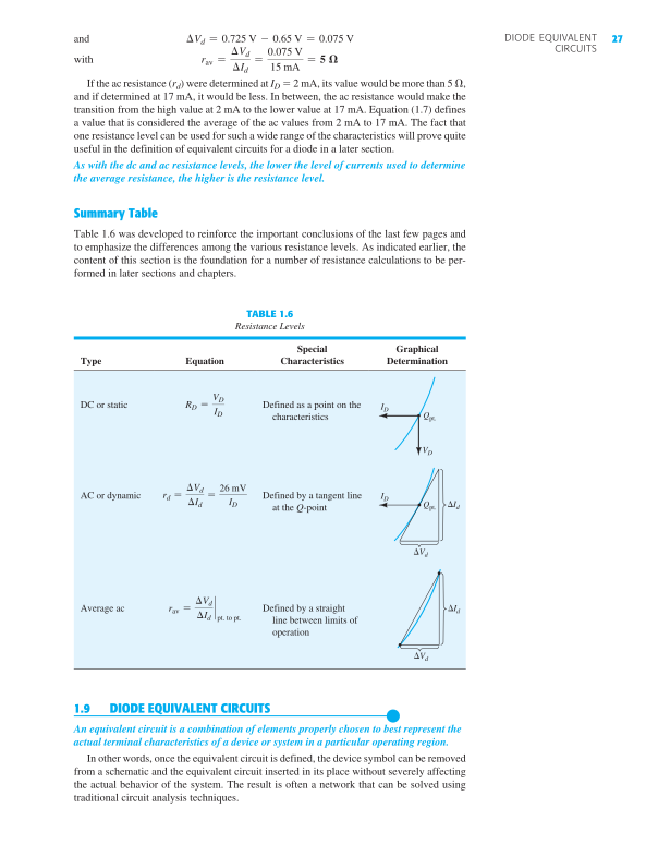
27DIODE EQUIVALENTCIRCUITSandVd = 0.725 V - 0.65 V = 0.075 Vwithrav = VdId= 0.075 V15 mA = 5If the ac resistance ( r d ) were determined at I D 2 mA, its value would be more than 5 ,and if determined at 17 mA, it would be less. In between, the ac resistance would make thetransition from the high value at 2 mA to the lower value at 17 mA. Equation (1.7) definesa value that is considered the average of the ac values from 2 mA to 17 mA. The fact thatone resistance level can be used for such a wide range of the characteristics will prove quiteuseful in the definition of equivalent circuits for a diode in a later section.As with the dc and ac resistance levels, the lower the level of currents used to determinethe average resistance, the higher is the resistance level.Summary TableTable 1.6 was developed to reinforce the important conclusions of the last few pages andto emphasize the differences among the various resistance levels. As indicated earlier, thecontent of this section is the foundation for a number of resistance calculations to be per-formed in later sections and chapters.TABLE 1.6Resistance LevelsTypeEquationSpecialCharacteristicsGraphicalDeterminationDC or staticRD = VDIDDefined as a point on thecharacteristicsAC or dynamicrd = VdId= 26 mVIDDefined by a tangent lineat the Q -pointAverage acrav = VdId`pt. to pt.Defined by a straightline between limits ofoperationIDVDQpt.IDVdIdQpt.VdId1.9DIODE EQUIVALENT CIRCUITS●An equivalent circuit is a combination of elements properly chosen to best represent theactual terminal characteristics of a device or system in a particular operating region.In other words, once the equivalent circuit is defined, the device symbol can be removedfrom a schematic and the equivalent circuit inserted in its place without severely affectingthe actual behavior of the system. The result is often a network that can be solved usingtraditional circuit analysis techniques.
textbook p. 27PDF p. 48
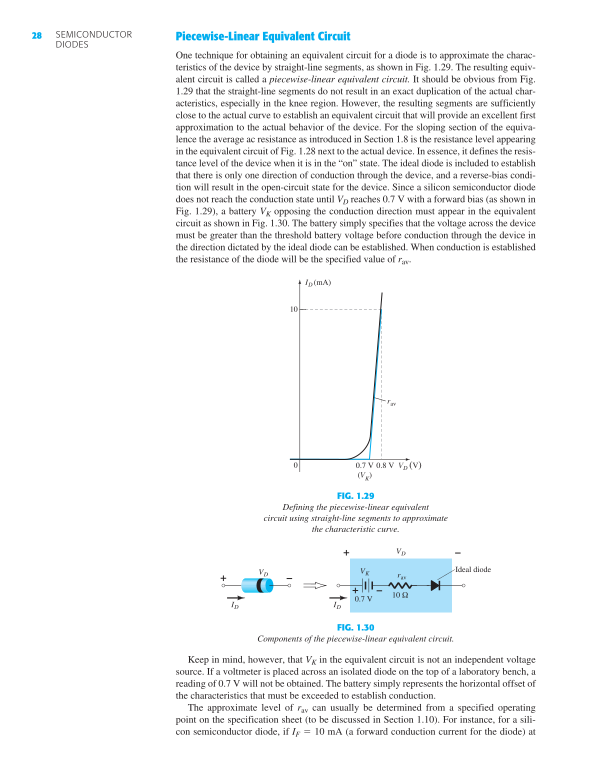
SEMICONDUCTORDIODES28Piecewise-Linear Equivalent CircuitOne technique for obtaining an equivalent circuit for a diode is to approximate the charac-teristics of the device by straight-line segments, as shown in Fig. 1.29 . The resulting equiv-alent circuit is called a piecewise-linear equivalent circuit. It should be obvious from Fig.1.29 that the straight-line segments do not result in an exact duplication of the actual char-acteristics, especially in the knee region. However, the resulting segments are sufficientlyclose to the actual curve to establish an equivalent circuit that will provide an excellent firstapproximation to the actual behavior of the device. For the sloping section of the equiva-lence the average ac resistance as introduced in Section 1.8 is the resistance level appearingin the equivalent circuit of Fig. 1.28 next to the actual device. In essence, it defines the resis-tance level of the device when it is in the “on” state. The ideal diode is included to establishthat there is only one direction of conduction through the device, and a reverse-bias condi-tion will result in the open-circuit state for the device. Since a silicon semiconductor diodedoes not reach the conduction state until V D reaches 0.7 V with a forward bias (as shown inFig. 1.29 ), a battery V K opposing the conduction direction must appear in the equivalentcircuit as shown in Fig. 1.30 . The battery simply specifies that the voltage across the devicemust be greater than the threshold battery voltage before conduction through the device inthe direction dictated by the ideal diode can be established. When conduction is establishedthe resistance of the diode will be the specified value of r av .1000.7 V(VK)0.8 V VD (V)ravI (mA)DIFIG. 1.29Defining the piecewise-linear equivalentcircuit using straight-line segments to approximatethe characteristic curve.DVDI+–avrKV0.7 V10 ΩDVIdeal diode++––DIFIG. 1.30Components of the piecewise-linear equivalent circuit.Keep in mind, however, that V K in the equivalent circuit is not an independent voltagesource. If a voltmeter is placed across an isolated diode on the top of a laboratory bench, areading of 0.7 V will not be obtained. The battery simply represents the horizontal offset ofthe characteristics that must be exceeded to establish conduction.The approximate level of r av can usually be determined from a specified operatingpoint on the specification sheet (to be discussed in Section 1.10 ). For instance, for a sili-con semiconductor diode, if I F 10 mA (a forward conduction current for the diode) at
textbook p. 28PDF p. 49
29DIODE EQUIVALENTCIRCUITSV D 0.8 V, we know that for silicon a shift of 0.7 V is required before the characteristicsrise, and we obtainrav = VdId`pt. to pt.= 0.8 V - 0.7 V10 mA - 0 mA = 0.1 V10 mA = 10as obtained for Fig. 1.29 .If the characteristics or specification sheet for a diode is not available the resistance r avcan be approximated by the ac resistance r d .Simplified Equivalent CircuitFor most applications, the resistance r av is sufficiently small to be ignored in comparison tothe other elements of the network. Removing r av from the equivalent circuit is the same asimplying that the characteristics of the diode appear as shown in Fig. 1.31 . Indeed, thisapproximation is frequently employed in semiconductor circuit analysis as demonstrated inChapter 2 . The reduced equivalent circuit appears in the same figure. It states that a forward-biased silicon diode in an electronic system under dc conditions has a drop of 0.7 V acrossit in the conduction state at any level of diode current (within rated values, of course).–ΩDVDI0KV = 0.7 Vavr= 0DI+DVIdeal diodeKV = 0.7 V+–FIG. 1.31Simplified equivalent circuit for the silicon semiconductor diode.FIG. 1.32Ideal diode and its characteristics.Ideal Equivalent CircuitNow that r av has been removed from the equivalent circuit, let us take the analysis a stepfurther and establish that a 0.7-V level can often be ignored in comparison to the appliedvoltage level. In this case the equivalent circuit will be reduced to that of an ideal diode asshown in Fig. 1.32 with its characteristics. In Chapter 2 we will see that this approximationis often made without a serious loss in accuracy.In industry a popular substitution for the phrase “diode equivalent circuit” is diode model —a model by definition being a representation of an existing device, object, system, and so on.In fact, this substitute terminology will be used almost exclusively in the chapters to follow.Summary TableFor clarity, the diode models employed for the range of circuit parameters and applicationsare provided in Table 1.7 with their piecewise-linear characteristics. Each will be investi-gated in greater detail in Chapter 2 . There are always exceptions to the general rule, but it
textbook p. 29PDF p. 50
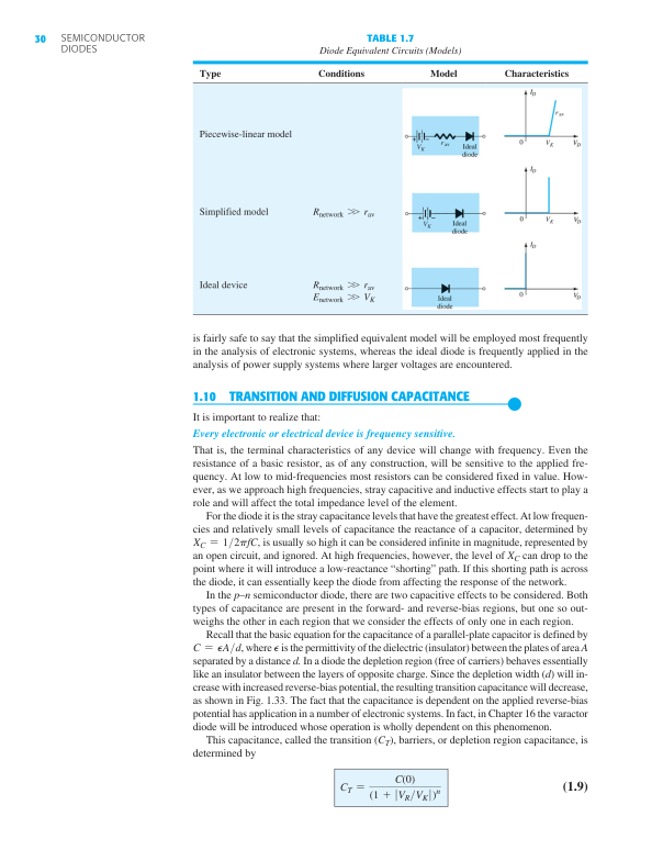
SEMICONDUCTORDIODES30is fairly safe to say that the simplified equivalent model will be employed most frequentlyin the analysis of electronic systems, whereas the ideal diode is frequently applied in theanalysis of power supply systems where larger voltages are encountered.1.10 TRANSITION AND DIFFUSION CAPACITANCE●It is important to realize that:Every electronic or electrical device is frequency sensitive.That is, the terminal characteristics of any device will change with frequency. Even theresistance of a basic resistor, as of any construction, will be sensitive to the applied fre-quency. At low to mid-frequencies most resistors can be considered fixed in value. How-ever, as we approach high frequencies, stray capacitive and inductive effects start to play arole and will affect the total impedance level of the element.For the diode it is the stray capacitance levels that have the greatest effect. At low frequen-cies and relatively small levels of capacitance the reactance of a capacitor, determined byXC = 1>2pfC, is usually so high it can be considered infinite in magnitude, represented byan open circuit, and ignored. At high frequencies, however, the level of X C can drop to thepoint where it will introduce a low-reactance “shorting” path. If this shorting path is acrossthe diode, it can essentially keep the diode from affecting the response of the network.In the p – n semiconductor diode, there are two capacitive effects to be considered. Bothtypes of capacitance are present in the forward- and reverse-bias regions, but one so out-weighs the other in each region that we consider the effects of only one in each region.Recall that the basic equation for the capacitance of a parallel-plate capacitor is defined byC = PA>d, where P is the permittivity of the dielectric (insulator) between the plates of area Aseparated by a distance d. In a diode the depletion region (free of carriers) behaves essentiallylike an insulator between the layers of opposite charge. Since the depletion width ( d ) will in-crease with increased reverse-bias potential, the resulting transition capacitance will decrease,as shown in Fig. 1.33 . The fact that the capacitance is dependent on the applied reverse-biaspotential has application in a number of electronic systems. In fact, in Chapter 16 the varactordiode will be introduced whose operation is wholly dependent on this phenomenon.This capacitance, called the transition ( C T ), barriers, or depletion region capacitance, isdetermined byCT =C(0)(1 + VR>VK )n(1.9)TABLE 1.7Diode Equivalent Circuits (Models)TypeConditionsModelCharacteristicsPiecewise-linear modelSimplified modelRnetwork W ravIdeal deviceRnetwork W ravEnetwork W VKVKVKVKVK+–+–
textbook p. 30PDF p. 51
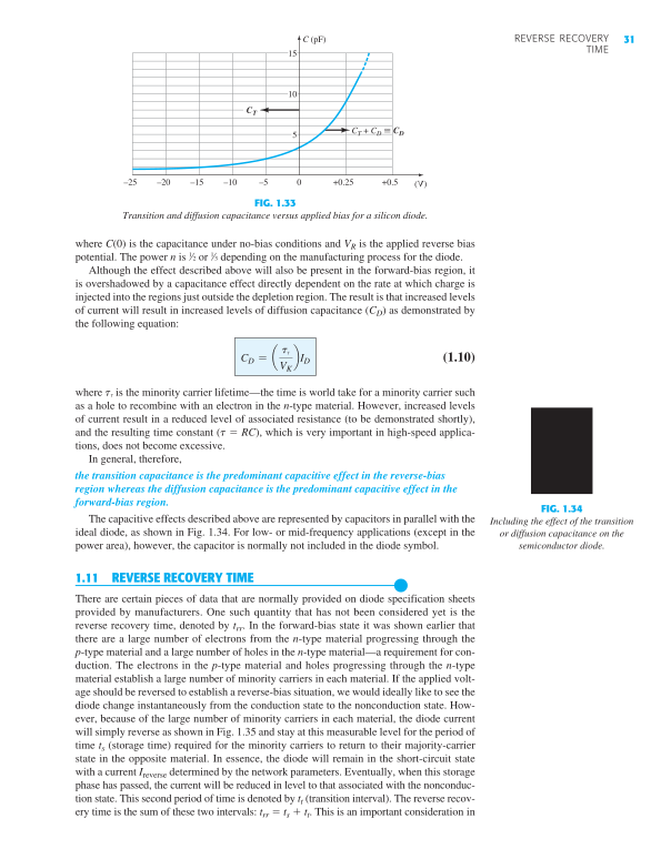
31REVERSE RECOVERYTIMEwhere C (0) is the capacitance under no-bias conditions and V R is the applied reverse biaspotential. The power n is 1⁄2 or 1⁄3 depending on the manufacturing process for the diode.Although the effect described above will also be present in the forward-bias region, itis overshadowed by a capacitance effect directly dependent on the rate at which charge isinjected into the regions just outside the depletion region. The result is that increased levelsof current will result in increased levels of diffusion capacitance ( C D ) as demonstrated bythe following equation:CD = a tVKbID(1.10)where t T is the minority carrier lifetime—the time is world take for a minority carrier suchas a hole to recombine with an electron in the n -type material. However, increased levelsof current result in a reduced level of associated resistance (to be demonstrated shortly),and the resulting time constant (t RC ), which is very important in high-speed applica-tions, does not become excessive.In general, therefore,the transition capacitance is the predominant capacitive effect in the reverse-biasregion whereas the diffusion capacitance is the predominant capacitive effect in theforward-bias region.The capacitive effects described above are represented by capacitors in parallel with theideal diode, as shown in Fig. 1.34 . For low- or mid-frequency applications (except in thepower area), however, the capacitor is normally not included in the diode symbol.1.11 REVERSE RECOVERY TIME●There are certain pieces of data that are normally provided on diode specification sheetsprovided by manufacturers. One such quantity that has not been considered yet is thereverse recovery time, denoted by t rr . In the forward-bias state it was shown earlier thatthere are a large number of electrons from the n -type material progressing through thep -type material and a large number of holes in the n -type material—a requirement for con-duction. The electrons in the p -type material and holes progressing through the n -typematerial establish a large number of minority carriers in each material. If the applied volt-age should be reversed to establish a reverse-bias situation, we would ideally like to see thediode change instantaneously from the conduction state to the nonconduction state. How-ever, because of the large number of minority carriers in each material, the diode currentwill simply reverse as shown in Fig. 1.35 and stay at this measurable level for the period oftime t s (storage time) required for the minority carriers to return to their majority-carrierstate in the opposite material. In essence, the diode will remain in the short-circuit statewith a current I reverse determined by the network parameters. Eventually, when this storagephase has passed, the current will be reduced in level to that associated with the nonconduc-tion state. This second period of time is denoted by t t (transition interval). The reverse recov-ery time is the sum of these two intervals: t rr t s t t . This is an important consideration in0+0.25+0.5510152025–––––(V)C51015TC(pF)CT + CD CDFIG. 1.33Transition and diffusion capacitance versus applied bias for a silicon diode.FIG. 1.34Including the effect of the transitionor diffusion capacitance on thesemiconductor diode.T
textbook p. 31PDF p. 52
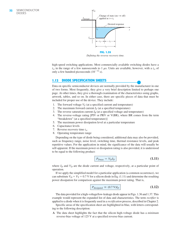
SEMICONDUCTORDIODES32high-speed switching applications. Most commercially available switching diodes have at rr in the range of a few nanoseconds to 1 ms. Units are available, however, with a t rr ofonly a few hundred picoseconds (10 12 s).1.12 DIODE SPECIFICATION SHEETS●Data on specific semiconductor devices are normally provided by the manufacturer in oneof two forms. Most frequently, they give a very brief description limited to perhaps onepage. At other times, they give a thorough examination of the characteristics using graphs,artwork, tables, and so on. In either case, there are specific pieces of data that must beincluded for proper use of the device. They include:1. The forward voltage V F (at a specified current and temperature)2. The maximum forward current I F (at a specified temperature)3. The reverse saturation current I R (at a specified voltage and temperature)4. The reverse-voltage rating [PIV or PRV or V(BR), where BR comes from the term“breakdown” (at a specified temperature)]5. The maximum power dissipation level at a particular temperature6. Capacitance levels7. Reverse recovery time t rr8. Operating temperature rangeDepending on the type of diode being considered, additional data may also be provided,such as frequency range, noise level, switching time, thermal resistance levels, and peakrepetitive values. For the application in mind, the significance of the data will usually beself-apparent. If the maximum power or dissipation rating is also provided, it is understoodto be equal to the following product:PDmax = VDID(1.11)where I D and V D are the diode current and voltage, respectively, at a particular point ofoperation.If we apply the simplified model for a particular application (a common occurrence), wecan substitute V D V T 0.7 V for a silicon diode in Eq. (1.11) and determine the resultingpower dissipation for comparison against the maximum power rating. That is,Pdissipated (0.7 V)ID(1.12)The data provided for a high-voltage/low-leakage diode appear in Figs. 1.36 and 1.37 . Thisexample would represent the expanded list of data and characteristics. The term rectifier isapplied to a diode when it is frequently used in a rectification process, described in Chapter 2 .Specific areas of the specification sheet are highlighted in blue, with letters correspond-ing to the following description:A The data sheet highlights the fact that the silicon high-voltage diode has a minimumreverse-bias voltage of 125 V at a specified reverse-bias current.DItforwardIreverseIChange of state (on off)applied at t = tt1tDesired response1tstttrrtFIG. 1.35Defining the reverse recovery time.
textbook p. 32PDF p. 53
33DIODE SPECIFICATIONSHEETSB Note the wide range of temperature operation. Always be aware that data sheets typi-cally use the centigrade scale, with 200°C 392°F and 65°C 85°F.C The maximum power dissipation level is given by PD = VDID = 500 mW = 0.5 W.The effect of the linear derating factor of 3.33 mW/°C is demonstrated in Fig. 1.37a .Once the temperature exceeds 25°C the maximum power rating will drop by 3.33 mWfor each 1°C increase in temperature. At a temperature of 100°C, which is the boilingpoint of water, the maximum power rating has dropped to one half of its original value.An initial temperature of 25°C is typical inside a cabinet containing operating elec-tronic equipment in a low-power situation.D The maximum sustainable current is 500 mA. The plot of Fig. 1.37b reveals that theforward current at 0.5 V is about 0.01 mA, but jumps to 1 mA (100 times greater) atabout 0.65 V. At 0.8 V the current is more than 10 mA, and just above 0.9 V it is close5.0DIFFUSED SILICON PLANARFIG. 1.36Electrical characteristics of a high-voltage, low-leakage diode.
textbook p. 33PDF p. 54
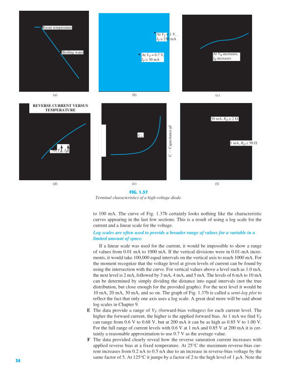
to 100 mA. The curve of Fig. 1.37b certainly looks nothing like the characteristiccurves appearing in the last few sections. This is a result of using a log scale for thecurrent and a linear scale for the voltage.Log scales are often used to provide a broader range of values for a variable in alimited amount of space.If a linear scale was used for the current, it would be impossible to show a rangeof values from 0.01 mA to 1000 mA. If the vertical divisions were in 0.01-mA incre-ments, it would take 100,000 equal intervals on the vertical axis to reach 1000 mA. Forthe moment recognize that the voltage level at given levels of current can be found byusing the intersection with the curve. For vertical values above a level such as 1.0 mA,the next level is 2 mA, followed by 3 mA, 4 mA, and 5 mA. The levels of 6 mA to 10 mAcan be determined by simply dividing the distance into equal intervals (not the truedistribution, but close enough for the provided graphs). For the next level it would be10 mA, 20 mA, 30 mA, and so on. The graph of Fig. 1.37b is called a semi-log plot toreflect the fact that only one axis uses a log scale. A great deal more will be said aboutlog scales in Chapter 9 .E The data provide a range of V F (forward-bias voltages) for each current level. Thehigher the forward current, the higher is the applied forward bias. At 1 mA we find V Fcan range from 0.6 V to 0.68 V, but at 200 mA it can be as high as 0.85 V to 1.00 V.For the full range of current levels with 0.6 V at 1 mA and 0.85 V at 200 mA it is cer-tainly a reasonable approximation to use 0.7 V as the average value.F The data provided clearly reveal how the reverse saturation current increases withapplied reverse bias at a fixed temperature. At 25°C the maximum reverse-bias cur-rent increases from 0.2 nA to 0.5 nA due to an increase in reverse-bias voltage by thesame factor of 5. At 125°C it jumps by a factor of 2 to the high level of 1 mA. Note the(a)(c)(d)(e)(f)(b)C Capacitance-pfRoom temperatureBoiling waterAt VF = 1 V,IF ≅ 250 mAAt VF = 0.7 V,IF ≅ 30 mAAt VR increases,IR increasesCT30 mA, RD ≅ 21 mA, RD ≅ 50REVERSE CURRENT VERSUSTEMPERATUREAs TA , IRFIG. 1.37Terminal characteristics of a high-voltage diode.34
textbook p. 34PDF p. 55
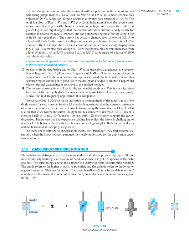
35SEMICONDUCTOR DIODENOTATIONextreme change in reverse saturation current with temperature as the maximum cur-rent rating jumps from 0.2 nA at 25°C to 500 nA at 125°C (at a fixed reverse-biasvoltage of 20 V). A similar increase occurs at a reverse-bias potential of 100 V. Thesemi-log plots of Figs. 1.37c and 1.37d provide an indication of how the reverse satu-ration current changes with changes in reverse voltage and temperature. At firstglance Fig. 1.37c might suggest that the reverse saturation current is fairly steady forchanges in reverse voltage. However, this can sometimes be the effect of using a logscale for the vertical axis. The current has actually changed from a level of 0.2 nA toa level of 0.7 nA for the range of voltages representing a change of almost 6 to 1. Thedramatic effect of temperature on the reverse saturation current is clearly displayed inFig. 1.37d . At a reverse-bias voltage of 125 V the reverse-bias current increases froma level of about 1 nA at 25°C to about 1 mA at 150°C, an increase of a factor of 1000over the initial value.Temperature and applied reverse bias are very important factors in designs sensitiveto the reverse saturation current.G As shown in the data listing and on Fig. 1.37e , the transition capacitance at a reverse-bias voltage of 0 V is 5 pF at a test frequency of 1 MHz. Note the severe change incapacitance level as the reverse-bias voltage is increased. As mentioned earlier, thissensitive region can be put to good use in the design of a device (Varactor; Chapter 16 )whose terminal capacitance is sensitive to the applied voltage.H The reverse recovery time is 3 ms for the test conditions shown. This is not a fast timefor some of the current high-performance systems in use today. However, for a varietyof low- and mid-frequency applications it is acceptable.The curves of Fig. 1.37f provide an indication of the magnitude of the ac resistance of thediode versus forward current. Section 1.8 clearly demonstrated that the dynamic resistanceof a diode decreases with increase in current. As we go up the current axis of Fig. 1.37f itis clear that if we follow the curve, the dynamic resistance will decrease. At 0.1 mA it isclose to 1 k ; at 10 mA, 10 ; and at 100 mA, only 1 ; this clearly supports the earlierdiscussion. Unless one has had experience reading log scales, the curve is challenging toread for levels between those indicated because it is a log–log plot . Both the vertical axisand the horizontal axis employ a log scale.The more one is exposed to specification sheets, the “friendlier” they will become, es-pecially when the impact of each parameter is clearly understood for the application underinvestigation.1.13 SEMICONDUCTOR DIODE NOTATION●The notation most frequently used for semiconductor diodes is provided in Fig. 1.38 . Formost diodes any marking such as a dot or band, as shown in Fig. 1.38 , appears at the cath-ode end. The terminology anode and cathode is a carryover from vacuum-tube notation.The anode refers to the higher or positive potential, and the cathode refers to the lower ornegative terminal. This combination of bias levels will result in a forward-bias or “on”condition for the diode. A number of commercially available semiconductor diodes appearin Fig. 1.39 .or •, K, etc.AnodeCathodepnFIG. 1.38Semiconductor diode notation.
textbook p. 35PDF p. 56
1.14 DIODE TESTING●The condition of a semiconductor diode can be determined quickly using (1) a digital dis-play meter (DDM) with a diode checking function , (2) the ohmmeter section of a multime-ter, or (3) a curve tracer.Diode Checking FunctionA digital display meter with a diode checking capability appears in Fig. 1.40 . Note thesmall diode symbol at the top right of the rotating dial. When set in this position andhooked up as shown in Fig. 1.41a , the diode should be in the “on” state and the display willprovide an indication of the forward-bias voltage such as 0.67 V (for Si). The meter has aninternal constant-current source (about 2 mA) that will define the voltage level as indicatedin Fig. 1.41b . An OL indication with the hookup of Fig. 1.41a reveals an open (defective)diode. If the leads are reversed, an OL indication should result due to the expected open-circuit equivalence for the diode. In general, therefore, an OL indication in both directionsis an indication of an open or defective diode.General purpose diodeBeam lead pin diodeFlat chip surface mount diodePower diodeSurface mount high-power PIN diodePower (stud) diodeFIG. 1.39Various types of junction diodes.Power (disc, puck) diodePower (planar) diodeFIG. 1.40Digital display meter. (Courtesy ofB&K Precision Corporation.)(a) (b)Red lead(VΩ)Black lead(COM)FIG. 1.41Checking a diode in the forward-bias state.Ohmmeter TestingIn Section 1.8 we found that the forward-bias resistance of a semiconductor diode is quitelow compared to the reverse-bias level. Therefore, if we measure the resistance of a diode36
textbook p. 36PDF p. 57
37DIODE TESTINGusing the connections indicated in Fig. 1.42 , we can expect a relatively low level. The result-ing ohmmeter indication will be a function of the current established through the diode by theinternal battery (often 1.5 V) of the ohmmeter circuit. The higher the current, the lower is theresistance level. For the reverse-bias situation the reading should be quite high, requiring ahigh resistance scale on the meter, as indicated in Fig. 1.42b . A high resistance reading inboth directions indicates an open (defective-device) condition, whereas a very low resis-tance reading in both directions will probably indicate a shorted device.Curve TracerThe curve tracer of Fig. 1.43 can display the characteristics of a host of devices, includingthe semiconductor diode. By properly connecting the diode to the test panel at the bottomcenter of the unit and adjusting the controls, one can obtain the display of Fig. 1.44 . Notethat the vertical scaling is 1 mA/div, resulting in the levels indicated. For the horizontal axisthe scaling is 100 mV/div, resulting in the voltage levels indicated. For a 2-mA level asdefined for a DDM, the resulting voltage would be about 625 mV 0.625 V. Although theinstrument initially appears quite complex, the instruction manual and a few moments ofexposure will reveal that the desired results can usually be obtained without an excessiveamount of effort and time. The display of the instrument will appear on more than one occa-sion in the chapters to follow as we investigate the characteristics of the variety of devices.+–(Ohmmeter)Relatively low RRed lead(V )Black lead(COM)(a)+–Relatively high RRed lead(V )Black lead(COM)(b)FIG. 1.42Checking a diode with anohmmeter.FIG. 1.43Curve tracer. (© Agilent Technologies, Inc. Reproduced withPermission, Courtesy of Agilent Technologies, Inc.)FIG. 1.44Curve tracer response to IN4007 silicon diode.
textbook p. 37PDF p. 58
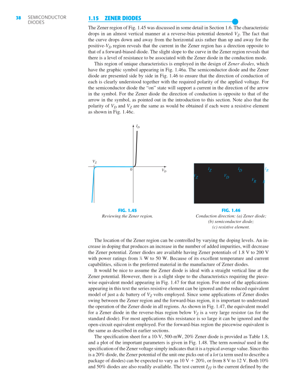
SEMICONDUCTORDIODES381.15 ZENER DIODES●The Zener region of Fig. 1.45 was discussed in some detail in Section 1.6 . The characteristicdrops in an almost vertical manner at a reverse-bias potential denoted V Z . The fact thatthe curve drops down and away from the horizontal axis rather than up and away for thepositive- V D region reveals that the current in the Zener region has a direction opposite tothat of a forward-biased diode. The slight slope to the curve in the Zener region reveals thatthere is a level of resistance to be associated with the Zener diode in the conduction mode.This region of unique characteristics is employed in the design of Zener diodes , whichhave the graphic symbol appearing in Fig. 1.46a . The semiconductor diode and the Zenerdiode are presented side by side in Fig. 1.46 to ensure that the direction of conduction ofeach is clearly understood together with the required polarity of the applied voltage. Forthe semiconductor diode the “on” state will support a current in the direction of the arrowin the symbol. For the Zener diode the direction of conduction is opposite to that of thearrow in the symbol, as pointed out in the introduction to this section. Note also that thepolarity of V D and V Z are the same as would be obtained if each were a resistive elementas shown in Fig. 1.46c .IDVDVZ0FIG. 1.45Reviewing the Zener region.VZVDVRIZIDIR(a) (b) (c)RFIG. 1.46Conduction direction: (a) Zener diode;(b) semiconductor diode;(c) resistive element.The location of the Zener region can be controlled by varying the doping levels. An in-crease in doping that produces an increase in the number of added impurities, will decreasethe Zener potential. Zener diodes are available having Zener potentials of 1.8 V to 200 Vwith power ratings from 1⁄4 W to 50 W. Because of its excellent temperature and currentcapabilities, silicon is the preferred material in the manufacture of Zener diodes.It would be nice to assume the Zener diode is ideal with a straight vertical line at theZener potential. However, there is a slight slope to the characteristics requiring the piece-wise equivalent model appearing in Fig. 1.47 for that region. For most of the applicationsappearing in this text the series resistive element can be ignored and the reduced equivalentmodel of just a dc battery of V Z volts employed. Since some applications of Zener diodesswing between the Zener region and the forward-bias region, it is important to understandthe operation of the Zener diode in all regions. As shown in Fig. 1.47 , the equivalent modelfor a Zener diode in the reverse-bias region below V Z is a very large resistor (as for thestandard diode). For most applications this resistance is so large it can be ignored and theopen-circuit equivalent employed. For the forward-bias region the piecewise equivalent isthe same as described in earlier sections.The specification sheet for a 10-V, 500-mW, 20% Zener diode is provided as Table 1.8 ,and a plot of the important parameters is given in Fig. 1.48 . The term nominal used in thespecification of the Zener voltage simply indicates that it is a typical average value. Since thisis a 20% diode, the Zener potential of the unit one picks out of a lot (a term used to describe apackage of diodes) can be expected to vary as 10 V 20%, or from 8 V to 12 V. Both 10%and 50% diodes are also readily available. The test current I ZT is the current defined by the
textbook p. 38PDF p. 59
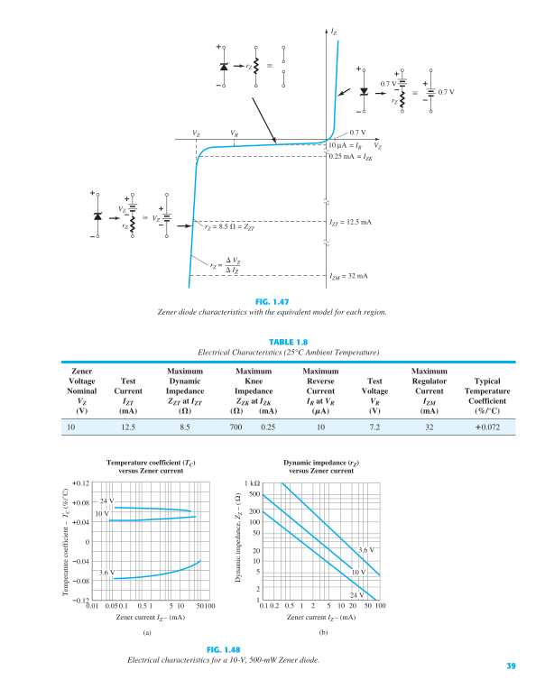
+–10 μA = IR0.25 mA = IZKIZT = 12.5 mArZ = 8.5 = ZZTrZ =IZM = 32 mAVZVZVRIZ+–VZVZIZ0.7 V0.7 V0.7 VrZ+–VZrZ+–+–+–rZ+–FIG. 1.47Zener diode characteristics with the equivalent model for each region.TABLE 1.8Electrical Characteristics (25°C Ambient Temperature)ZenerVoltageNominalV Z(V)TestCurrentI ZT(mA)MaximumDynamicImpedanceZ ZT at I ZT( )MaximumKneeImpedanceZ ZK at I ZK( ) (mA)MaximumReverseCurrentI R at V R(MA)TestVoltageV R(V)MaximumRegulatorCurrentI ZM(mA)TypicalTemperatureCoefficient(%/°C)1012.58.57000.25107.2320.072–0.120.01Temperature coefficient – (%/˚C)Temperature coefficient (TC)versus Zener current–0.08–0.040+0.04+0.08Zener current IZ – (mA)0.11101000.050.5550CT(a)3.6 V10 V24 V+0.1210.1Dynamic impedance (rZ)versus Zener currentDynamic impedance, ZZ – ( )Ω251020501002005001 k Ω20.2550 100101200.524 V(b)3.6 VZener current IZ – (mA)10 VFIG. 1.48Electrical characteristics for a 10-V, 500-mW Zener diode.39
textbook p. 39PDF p. 60
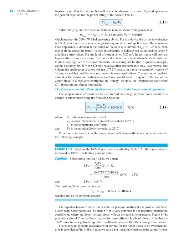
SEMICONDUCTORDIODES401⁄4-power level. It is the current that will define the dynamic resistance Z ZT and appears inthe general equation for the power rating of the device. That is,PZmax = 4IZTVZ(1.13)Substituting I ZT into the equation with the nominal Zener voltage results inPZmax = 4IZTVZ = 4(12.5 mA)(10 V) = 500 mWwhich matches the 500-mW label appearing above. For this device the dynamic resistanceis 8.5 , which is usually small enough to be ignored in most applications. The maximumknee impedance is defined at the center of the knee at a current of I ZK 0.25 mA. Notethat in all the above the letter T is used in subscripts to indicate test values and the letter Kto indicate knee values. For any level of current below 0.25 mA the resistance will only getlarger in the reverse-bias region. The knee value therefore reveals when the diode will startto show very high series resistance elements that one may not be able to ignore in an appli-cation. Certainly 500 0.5 k may be a level that can come into play. At a reverse-biasvoltage the application of a test voltage of 7.2 V results in a reverse saturation current of10 mA, a level that could be of some concern in some applications. The maximum regulatorcurrent is the maximum continuous current one would want to support in the use of theZener diode in a regulator configuration. Finally, we have the temperature coefficient( T C ) in percent per degree centigrade.The Zener potential of a Zener diode is very sensitive to the temperature of operation.The temperature coefficient can be used to find the change in Zener potential due to achange in temperature using the following equation:TC = VZ>VZT1 - T0* 100%/ C (%/ C)(1.14)whereT 1 is the new temperature levelT 0 is room temperature in an enclosed cabinet (25°C)T C is the temperature coefficientandV Z is the nominal Zener potential at 25°C.To demonstrate the effect of the temperature coefficient on the Zener potential, considerthe following example.EXAMPLE 1.5 Analyze the 10-V Zener diode described by Table 1.7 if the temperature isincreased to 100°C (the boiling point of water).Solution: Substituting into Eq. (1.14), we obtainVZ = TCVZ100%(T1 - T0)= (0.072%/ C)(10 V)100%(100 C - 25 C)andVZ = 0.54 VThe resulting Zener potential is nowVZ = VZ + 0.54 V = 10.54 Vwhich is not an insignificant change.It is important to realize that in this case the temperature coefficient was positive. For Zenerdiodes with Zener potentials less than 5 V it is very common to see negative temperaturecoefficients, where the Zener voltage drops with an increase in temperature. Figure 1.48aprovides a plot of T versus Zener current for three different levels of diodes. Note that the3.6-V diode has a negative temperature coefficient, whereas the others have positive values.The change in dynamic resistance with current for the Zener diode in its avalanche re-gion is provided in Fig. 1.48b . Again, we have a log–log plot, which has to be carefully read.
textbook p. 40PDF p. 61
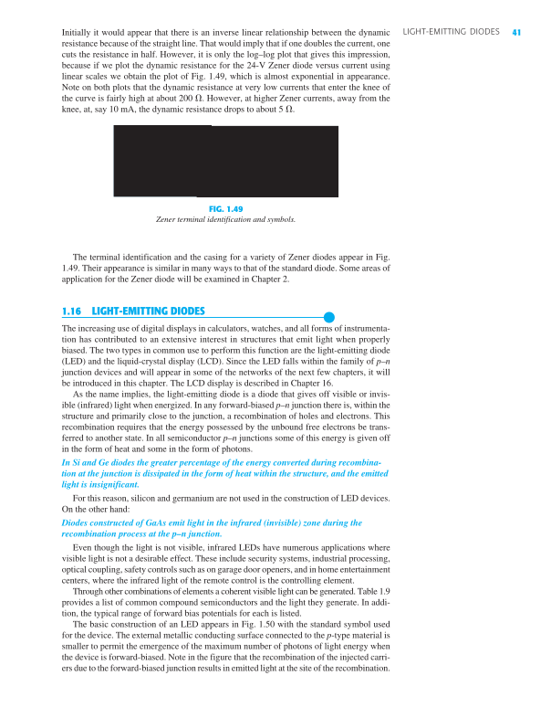
41LIGHT-EMITTING DIODESInitially it would appear that there is an inverse linear relationship between the dynamicresistance because of the straight line. That would imply that if one doubles the current, onecuts the resistance in half. However, it is only the log–log plot that gives this impression,because if we plot the dynamic resistance for the 24-V Zener diode versus current usinglinear scales we obtain the plot of Fig. 1.49 , which is almost exponential in appearance.Note on both plots that the dynamic resistance at very low currents that enter the knee ofthe curve is fairly high at about 200 . However, at higher Zener currents, away from theknee, at, say 10 mA, the dynamic resistance drops to about 5 .FIG. 1.49Zener terminal identification and symbols.The terminal identification and the casing for a variety of Zener diodes appear in Fig.1.49 . Their appearance is similar in many ways to that of the standard diode. Some areas ofapplication for the Zener diode will be examined in Chapter 2 .1.16 LIGHT-EMITTING DIODES●The increasing use of digital displays in calculators, watches, and all forms of instrumenta-tion has contributed to an extensive interest in structures that emit light when properlybiased. The two types in common use to perform this function are the light-emitting diode(LED) and the liquid-crystal display (LCD). Since the LED falls within the family of p – njunction devices and will appear in some of the networks of the next few chapters, it willbe introduced in this chapter. The LCD display is described in Chapter 16 .As the name implies, the light-emitting diode is a diode that gives off visible or invis-ible (infrared) light when energized. In any forward-biased p – n junction there is, within thestructure and primarily close to the junction, a recombination of holes and electrons. Thisrecombination requires that the energy possessed by the unbound free electrons be trans-ferred to another state. In all semiconductor p – n junctions some of this energy is given offin the form of heat and some in the form of photons.In Si and Ge diodes the greater percentage of the energy converted during recombina-tion at the junction is dissipated in the form of heat within the structure, and the emittedlight is insignificant.For this reason, silicon and germanium are not used in the construction of LED devices.On the other hand:Diodes constructed of GaAs emit light in the infrared (invisible) zone during therecombination process at the p–n junction.Even though the light is not visible, infrared LEDs have numerous applications wherevisible light is not a desirable effect. These include security systems, industrial processing,optical coupling, safety controls such as on garage door openers, and in home entertainmentcenters, where the infrared light of the remote control is the controlling element.Through other combinations of elements a coherent visible light can be generated. Table 1.9provides a list of common compound semiconductors and the light they generate. In addi-tion, the typical range of forward bias potentials for each is listed.The basic construction of an LED appears in Fig. 1.50 with the standard symbol usedfor the device. The external metallic conducting surface connected to the p -type material issmaller to permit the emergence of the maximum number of photons of light energy whenthe device is forward-biased. Note in the figure that the recombination of the injected carri-ers due to the forward-biased junction results in emitted light at the site of the recombination.
textbook p. 41PDF p. 62
SEMICONDUCTORDIODES42There will, of course, be some absorption of the packages of photon energy in the structureitself, but a very large percentage can leave, as shown in the figure.TABLE 1.9Light-Emitting DiodesColorConstructionTypical ForwardVoltage (V)AmberAlInGaP2.1BlueGaN5.0GreenGaP2.2OrangeGaAsP2.0RedGaAsP1.8WhiteGaN4.1YellowAlInGaP2.1(a)(b)FIG. 1.50(a) Process of electroluminescence in the LED; (b) graphic symbol.Just as different sounds have different frequency spectra (high-pitched sounds generallyhave high-frequency components, and low sounds have a variety of low-frequency compo-nents), the same is true for different light emissions.The frequency spectrum for infrared light extends from about 100 THz (T tera10 12 ) to 400 THz, with the visible light spectrum extending from about 400 to 750 THz.It is interesting to note that invisible light has a lower frequency spectrum than visiblelight.In general, when one talks about the response of electroluminescent devices, one refer-ences their wavelength rather than their frequency.The two quantities are related by the following equation:l = cf (m)(1.15)wherec 3 10 8 m/s (the speed of light in a vacuum)f frequency in Hertzl wavelength in meters.
textbook p. 42PDF p. 63
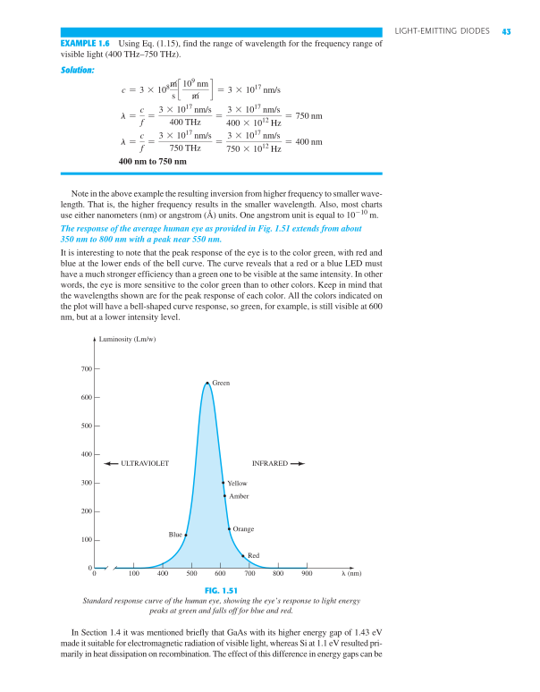
43LIGHT-EMITTING DIODESEXAMPLE 1.6 Using Eq. (1.15), find the range of wavelength for the frequency range ofvisible light (400 THz–750 THz).Solution:c = 3 * 108ms c 109 nmmd = 3 * 1017 nm/sl = cf = 3 * 1017 nm/s400 THz= 3 * 1017 nm/s400 * 1012 Hz= 750 nml = cf = 3 * 1017 nm/s750 THz= 3 * 1017 nm/s750 * 1012 Hz= 400 nm400 nm to 750 nmNote in the above example the resulting inversion from higher frequency to smaller wave-length. That is, the higher frequency results in the smaller wavelength. Also, most chartsuse either nanometers (nm) or angstrom (Å) units. One angstrom unit is equal to 10 10 m.The response of the average human eye as provided in Fig. 1.51 extends from about350 nm to 800 nm with a peak near 550 nm.It is interesting to note that the peak response of the eye is to the color green, with red andblue at the lower ends of the bell curve. The curve reveals that a red or a blue LED musthave a much stronger efficiency than a green one to be visible at the same intensity. In otherwords, the eye is more sensitive to the color green than to other colors. Keep in mind thatthe wavelengths shown are for the peak response of each color. All the colors indicated onthe plot will have a bell-shaped curve response, so green, for example, is still visible at 600nm, but at a lower intensity level.ULTRAVIOLETINFRAREDGreenYellowAmberOrangeRedLuminosity (Lm/w)70060050040030020010010040050060070080090000Blue(nm)FIG. 1.51Standard response curve of the human eye, showing the eye’s response to light energypeaks at green and falls off for blue and red.In Section 1.4 it was mentioned briefly that GaAs with its higher energy gap of 1.43 eVmade it suitable for electromagnetic radiation of visible light, whereas Si at 1.1 eV resulted pri-marily in heat dissipation on recombination. The effect of this difference in energy gaps can be
textbook p. 43PDF p. 64
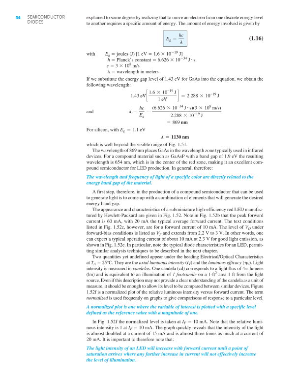
SEMICONDUCTORDIODES44explained to some degree by realizing that to move an electron from one discrete energy levelto another requires a specific amount of energy. The amount of energy involved is given byEg = hcl(1.16)withE g joules (J) [1 eV 1.6 10 19 J]h Planck’s constant 6.626 10 34 J # s.c 3 10 8 m/sl wavelength in metersIf we substitute the energy gap level of 1.43 eV for GaAs into the equation, we obtain thefollowing wavelength:1.43 eVc 1.6 * 10-19 J1 eVd = 2.288 * 10-19 Jandl = hcEg= (6.626 * 10-34 J # s)(3 * 108 m/s)2.288 * 10-19 J= 869 nmFor silicon, with Eg = 1.1 eVl = 1130 nmwhich is well beyond the visible range of Fig. 1.51.The wavelength of 869 nm places GaAs in the wavelength zone typically used in infrareddevices. For a compound material such as GaAsP with a band gap of 1.9 eV the resultingwavelength is 654 nm, which is in the center of the red zone, making it an excellent com-pound semiconductor for LED production. In general, therefore:The wavelength and frequency of light of a specific color are directly related to theenergy band gap of the material.A first step, therefore, in the production of a compound semiconductor that can be usedto generate light is to come up with a combination of elements that will generate the desiredenergy band gap.The appearance and characteristics of a subminiature high-efficiency red LED manufac-tured by Hewlett-Packard are given in Fig. 1.52 . Note in Fig. 1.52b that the peak forwardcurrent is 60 mA, with 20 mA the typical average forward current. The text conditionslisted in Fig. 1.52c , however, are for a forward current of 10 mA. The level of V D underforward-bias conditions is listed as V F and extends from 2.2 V to 3 V. In other words, onecan expect a typical operating current of about 10 mA at 2.3 V for good light emission, asshown in Fig. 1.52e . In particular, note the typical diode characteristics for an LED, permit-ting similar analysis techniques to be described in the next chapter.Two quantities yet undefined appear under the heading Electrical/Optical Characteristicsat T A 25°C. They are the axial luminous intensity ( I V ) and the luminous efficacy (h V ). Lightintensity is measured in candelas. One candela (cd) corresponds to a light flux of 4p lumens(lm) and is equivalent to an illumination of 1 footcandle on a 1-ft 2 area 1 ft from the lightsource. Even if this description may not provide a clear understanding of the candela as a unit ofmeasure, it should be enough to allow its level to be compared between similar devices. Figure1.52f is a normalized plot of the relative luminous intensity versus forward current. The termnormalized is used frequently on graphs to give comparisons of response to a particular level.A normalized plot is one where the variable of interest is plotted with a specific leveldefined as the reference value with a magnitude of one.In Fig. 1.52f the normalized level is taken at I F 10 mA. Note that the relative lumi-nous intensity is 1 at I F 10 mA. The graph quickly reveals that the intensity of the lightis almost doubled at a current of 15 mA and is almost three times as much at a current of20 mA. It is important to therefore note that:The light intensity of an LED will increase with forward current until a point ofsaturation arrives where any further increase in current will not effectively increasethe level of illumination.
textbook p. 44PDF p. 65
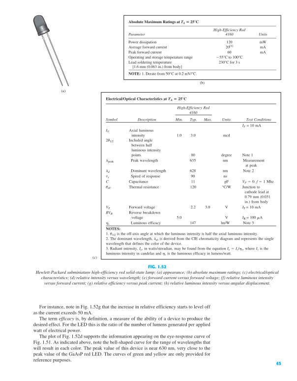
For instance, note in Fig. 1.52g that the increase in relative efficiency starts to level offas the current exceeds 50 mA.The term efficacy is, by definition, a measure of the ability of a device to produce thedesired effect. For the LED this is the ratio of the number of lumens generated per appliedwatt of electrical power.The plot of Fig. 1.52d supports the information appearing on the eye-response curve ofFig. 1.51 . As indicated above, note the bell-shaped curve for the range of wavelengths thatwill result in each color. The peak value of this device is near 630 nm, very close to thepeak value of the GaAsP red LED. The curves of green and yellow are only provided forreference purposes.(b)(a)Absolute Maximum Ratings at T A 25°CParameterHigh-Efficiency Red4160UnitsPower dissipation120mWAverage forward current20[1]mAPeak forward current60mAOperating and storage temperature range55°C to 100°CLead soldering temperature[1.6 mm (0.063 in.) from body]230°C for 3 sNOTE: 1. Derate from 50°C at 0.2 mV/°C.(c)Electrical/Optical Characteristics at T A 25°CHigh-Efficiency Red4160SymbolDescriptionMin.Typ.Max.UnitsTest ConditionsI F = 10 mAI VAxial luminousintensity1.03.0mcd2u 1/2Included anglebetween halfluminous intensitypoints80degreeNote 1l peakPeak wavelength635nmMeasurementat peakl dDominant wavelength628nmNote 2t sSpeed of response90nsCCapacitance11pFV F 0; f 1 Mhzu JCThermal resistance120°C/WJunction tocathode lead at0.79 mm (0.031in.) from bodyV FForward voltage2.23.0VI F = 10 mABV RReverse breakdownvoltage5.0VI R = 100 m Ah vLuminous efficacy147lm/WNote 3NOTES:1. u 1/2 is the off-axis angle at which the luminous intensity is half the axial luminous intensity.2. The dominant wavelength, l d , is derived from the CIE chromaticity diagram and represents the singlewavelength that defines the color of the device.3. Radiant intensity, I e , in watts/steradian, may be found from the equation I e I v /h v , where I v is theluminous intensity in candelas and h v is the luminous efficacy in lumens/watt.FIG. 1.52Hewlett-Packard subminiature high-efficiency red solid-state lamp: (a) appearance; (b) absolute maximum ratings; (c) electrical/opticalcharacteristics; (d) relative intensity versus wavelength; (e) forward current versus forward voltage; (f) relative luminous intensityversus forward current; (g) relative efficiency versus peak current; (h) relative luminous intensity versus angular displacement.45
textbook p. 45PDF p. 66
Figure 1.52h is a graph of light intensity versus angle measured from 0° (head on)to 90° (side view). Note that at 40° the intensity has already dropped to 50% of thehead-on intensity.One of the major concerns when using an LED is the reverse-bias breakdown voltage,which is typically between 3 V and 5 V (an occasional device has a 10-V level).This range of values is significantly less than that of a standard commercial diode,where it can extend to thousands of volts. As a result one has to be acutely aware of thissevere limitation in the design process. In the next chapter one protective approach will beintroduced.In the analysis and design of networks with LEDs it is helpful to have some idea of thevoltage and current levels to be expected.For many years the only colors available were green, yellow, orange, and red, permittingthe use of the average values of V F 2 V and I F 20 mA for obtaining an approximateoperating level.However, with the introduction of blue in the early 1990s and white in the late 1990s themagnitude of these two parameters has changed. For blue the average forward bias voltagecan be as high as 5 V, and for white about 4.1 V, although both have a typical operatingcurrent of 20 mA or more. In general, therefore:Assume an average forward-bias voltage of 5 V for blue and 4 V for white LEDs atcurrents of 20 mA to initiate an analysis of networks with these types of LEDs.Every once in a while a device is introduced that seems to open the door to a slue ofpossibilities. Such is the case with the introduction of white LEDs. The slow start for whiteLEDs is primarily due to the fact that it is not a primary color like green, blue, and red.Every other color that one requires, such as on a TV screen, can be generated from thesethree colors (as in virtually all monitors available today). Yes, the right combination ofthese three colors can give white—hard to believe, but it works. The best evidence is the(d)(f) (g)(h)(e)FIG. 1.52Continued.46
textbook p. 46PDF p. 67
47LIGHT-EMITTING DIODEShuman eye, which only has cones sensitive to red, green, and blue. The brain is responsiblefor processing the input and perceiving the “white” light and color we see in our everydaylives. The same reasoning was used to generate some of the first white LEDs, by combiningthe right proportions of a red, a green, and a blue LED in a single package. Today, however,most white LEDs are constructed of a blue gallium nitride LED below a film of yttrium-aluminum garnet (YAG) phosphor. When the blue light hits the phosphor, a yellow light isgenerated. The mix of this yellow emission with that of the central blue LED forms a whitelight—incredible, but true.Since most of the lighting for homes and offices is white light, we now have anotheroption to consider versus incandescent and fluorescent lighting. The rugged characteristicsof LED white light along with lifetimes that exceed 25,000 hours, clearly suggest thatthis will be a true competitor in the near future. Various companies are now providingreplacement LED bulbs for almost every possible application. Some have efficacy ratingsas high as 135.7 lumens per watt, far exceeding the 25 lumens per watt of a few yearsago. It is forecast that 7 W of power will soon be able to generate 1,000 lm of light, whichexceeds the illumination of a 60 W bulb and can run off four D cell batteries. Imaginethe same lighting with less than 1>8 the power requirement. At the present time entire of-fices, malls, street lighting, sporting facilities, and so on are being designed using solelyLED lighting. Recently, LEDs are the common choice for flashlights and many high-endautomobiles due to the sharp intensity at lower dc power requirements. The tube light ofFig. 1.53a replaces the standard fluorescent bulb typically found in the ceiling fixtures ofboth the home and industry. Not only do they draw 20% less energy while providing 25%additional light but they also last twice as long as a standard fluorescent bulb. The floodlight of Fig. 1.53b draws 1.7 watts for each 140 lumens of light resulting in an enormous90% savings in energy compared to the incandescent variety. The chandelier bulbs of Fig.1.53c have a lifetime of 50,000 hours and only draw 3 watts of power while generating200 lumens of light.(a)(c)(b)FIG. 1.53LED residential and commercial lighting.Before leaving the subject, let us look at a seven-segment digital display housed in atypical dual in-line integrated circuit package as shown in Fig. 1.54 . By energizing theproper pins with a typical 5-V dc level, a number of the LEDs can be energized and thedesired numeral displayed. In Fig. 1.54a the pins are defined by looking at the face ofthe display and counting counterclockwise from the top left pin. Most seven-segmentdisplays are either common-anode or common-cathode displays, with the term anodereferring to the defined positive side of each diode and the cathode referring to the nega-tive side. For the common-cathode option the pins have the functions listed in Fig. 1.54band appear as in Fig. 1.54c . In the common-cathode configuration all the cathodes areconnected together to form a common point for the negative side of each LED. Any LEDwith a positive 5 V applied to the anode or numerically numbered pin side will turn onand produce light for that segment. In Fig. 1.54c , 5 V has been applied to the terminalsthat generate the numeral 5. For this particular unit the average forward turn-on voltageis 2.1 V at a current of 10 mA.Various LED configurations are examined in the next chapter.
textbook p. 47PDF p. 68
SEMICONDUCTORDIODES481.17 SUMMARY●Important Conclusions and Concepts1. The characteristics of an ideal diode are a close match with those of a simple switchexcept for the important fact that an ideal diode can conduct in only one direction .2. The ideal diode is a short in the region of conduction and an open circuit in theregion of nonconduction.3. A semiconductor is a material that has a conductivity level somewhere between thatof a good conductor and that of an insulator.4. A bonding of atoms, strengthened by the sharing of electrons between neighboringatoms, is called covalent bonding.5. Increasing temperatures can cause a significant increase in the number of free elec-trons in a semiconductor material.6. Most semiconductor materials used in the electronics industry have negative tem-perature coefficients ; that is, the resistance drops with an increase in temperature.7. Intrinsic materials are those semiconductors that have a very low level of impurities ,whereas extrinsic materials are semiconductors that have been exposed to a dopingprocess .8. An n -type material is formed by adding donor atoms that have five valence electronsto establish a high level of relatively free electrons. In an n -type material, the electronis the majority carrier and the hole is the minority carrier.9. A p -type material is formed by adding acceptor atoms with three valence electrons toestablish a high level of holes in the material. In a p -type material, the hole is themajority carrier and the electron is the minority carrier.10. The region near the junction of a diode that has very few carriers is called the deple-tion region.11. In the absence of any externally applied bias, the diode current is zero.12. In the forward-bias region the diode current increases exponentially with increase involtage across the diode.afecgbd178145 V5 V 5 V5 V5 VComputer control0.630"0.803"1.0875"(a)(b)COMMON CATHODEPIN # FUNCTION1. Anode f2. ANODE g3. NO PIN4. COMMON CATHODE5. NO PIN6. ANODE e7. ANODE d8. ANODE c9. ANODE d10. NO PIN11. NO PIN12. COMMON CATHODE13. ANODE b14. ANODE a1234567141312111098(c)FIG. 1.54Seven-segment display: (a) face with pin idenfication; (b) pin function; (c) displaying the numeral 5.
textbook p. 48PDF p. 69
49COMPUTER ANALYSIS13. In the reverse-bias region the diode current is the very small reverse saturation cur-rent until Zener breakdown is reached and current will flow in the opposite directionthrough the diode.14. The reverse saturation current I s will just about double in magnitude for every 10-foldincrease in temperature.15. The dc resistance of a diode is determined by the ratio of the diode voltage and cur-rent at the point of interest and is not sensitive to the shape of the curve. The dc resis-tance decreases with increase in diode current or voltage.16. The ac resistance of a diode is sensitive to the shape of the curve in the region of inter-est and decreases for higher levels of diode current or voltage.17. The threshold voltage is about 0.7 V for silicon diodes and 0.3 V for germanium diodes.18. The maximum power dissipation level of a diode is equal to the product of the diodevoltage and current.19. The capacitance of a diode increases exponentially with increase in the forward-biasvoltage. Its lowest levels are in the reverse-bias region.20. The direction of conduction for a Zener diode is opposite to that of the arrow in thesymbol, and the Zener voltage has a polarity opposite to that of a forward-biased diode.21. Light emitting diodes (LEDs) emit light under forward-bias conditions but require 2V to 4 V for good emission.EquationsID = Is(eVD>nVT - 1) VT = kTq TK = TC + 273 k = 1.38 * 10-23 J>KVK 0.7 V (Si)VK 1.2 V (GaAs)VK 0.3 V (Ge)RD = VDIDrd = VdId= 26 mVIDrav = VdId`pt. to pt.PDmax = VD ID1.18 COMPUTER ANALYSIS●Two software packages designed to analyze electronic circuits will be introduced and appliedthroughout the text. They include Cadence OrCAD, version 16.3 ( Fig. 1.55 ), and Multi-sim, version 11.0.1 ( Fig. 1.56 ). The content was written with sufficient detail to ensure thatthe reader will not need to reference any other computer literature to apply both programs.FIG. 1.55Cadence OrCAD Design package version 16.3.(Photo by Dan Trudden/Pearson.)FIG. 1.56Multisim 11.0.1.(Photo by Dan Trudden/Pearson.)
textbook p. 49PDF p. 70

SEMICONDUCTORDIODES50Those of you who have used either program in the past will find that the changes are minorand appear primarily in the front end and in the generation of specific data and plots.The reason for including two programs stems from the fact that both are used throughoutthe educational community. You will find that the OrCAD software has a broader area ofinvestigation but the Multisim software generates displays that are a better match to theactual laboratory experience.The demo version of OrCAD is free from Cadence Design Systems, Inc., and can bedownloaded directly from the EMA Design Automation, Inc., web site, info@emaeda.com .Multisim must be purchased from the National Instruments Corporation using their website, ni.com/multisim.In previous editions, the OrCAD package was referred to as a PSpice program primarilybecause it is a subset of a more sophisticated version used extensively in industry calledSPICE . The result is the use of the term PSpice in the descriptions to follow when initiatingan analysis using the OrCAD software.The downloading process for each software package will now be introduced along withthe general appearance of the resulting screen.OrCADInstallation:Insert the OrCAD Release 16.3 DVD into the disk drive to open the Cadence OrCAD16.3 software screen.Select Demo Installation and the Preparing Setup dialog box will open, followed bythe message Welcome to the Installation Wizard for OrCAD 16.3 Demo. SelectNext, and the License Agreement dialog box opens. Choose I accept and selectNext , and the Choose Destination dialog box will open with Install OrCAD 16.3Demo Accept C:\OrCAD\OrCAD_16.3 Demo.Select Next , and the Start Copying Files dialog box opens. Choose Select again, andthe Ready to Install Program dialog box opens. Click Install , and the InstallingCrystal Report Xii box will appear. The Setup dialog box opens with the prompt:Setup status installs program . The Install Wizard is now installing the OrCAD16.3 Demo.At completion, a message will appear: Searching for and adding programs to theWindows firewall exception list. Generating indexes for Cadence Help. Thismay take some time.When the process has completed, select Finish and the Cadence OrCAD 16.3 screenwill appear. The software has been installed.Screen Icon: The screen icon can be established (if it does not appear automatically) byapplying the following sequence. START-All Programs-Cadence-OrCAD 16.3 Demo-OrCAD Capture CIS Demo, followed by a right-click of the mouse to obtain a listingwhere Send to is chosen, followed by Desktop (create shortcut). The OrCAD icon willthen appear on the screen and can be moved to the appropriate location.Folder Creation: Starting with the OrCAD opening screen, right-click on the Startoption at the bottom left of the screen. Then choose Explore followed by Hard Drive(C:). Then place the mouse on the folder listing, and a right-click will result in a listing inwhich New is an option. Choose New followed by Folder , and then type in OrCAD 11.3in the provided area of the screen, followed by a right-click of the mouse. A location for allthe files generated using OrCAD has now been established.MultisimInstallation:Insert the Multisim disk into the DVD disk drive to obtain the Autoplay dialog box.Then select Always do this for software and games , followed by the selection ofAuto-run to open the NI Circuit Design Suite 11.0 dialog box.
textbook p. 50PDF p. 71

51PROBLEMSEnter the full name to be used and provide the serial number. (The serial numberappears in the Certificate of Ownership document that came with the NI CircuitDesign Suite packet.)Selecting Next will result in the Destination Directory dialog box from which one willAccept the following: C:\Program Files(X86) National Instruments\. Select Nextto open the Features dialog box and then select NI Circuit Design Suite 11.0.1Education.Selecting Next will result in the Product Notification dialog box with a succeedingNext resulting in the License Agreement dialog box. A left-click of the mouse on Iaccept can then be followed by choosing Next to obtain the Start Installation dialogbox. Another left-click and the installation process begins, with the progress beingdisplayed. The process takes between 15 and 20 minutes.At the conclusion of the installation, you will be asked to install the NI Elvismx driverDVD . This time Cancel will be selected, and the NI Circuit Design Suite 11.0.1dialog box will appear with the following message: NI Circuit Design Suite 11.0.1has been installed. Click Finish , and the response will be to restart the computer tocomplete the operation. Select Restart , and the computer will shut down and start upagain, followed by the appearance of the Multisim Screen dialog box.Select Activate and then Activate through secure Internet connection , and the Acti-vation Wizard dialog box will open. Enter the serial number followed by Next toenter all the information into the NI Activation Wizard dialog box. Selecting Nextwill result in the option of Send me an email confirmation of this activation . Selectthis option and the message Product successfully activated will appear. SelectingFinish will complete the process.Screen Icon: The process described for the OrCAD program will produce the sameresults for Multisim.Folder Creation: Following the procedure introduced above for the OrCAD program, afolder labeled OrCAD 16.3 was established for the Multisim files.The computer section of the next chapter will cover the details of opening both theOrCAD and Multisim analysis packages, setting up a specific circuit, and generating avariety of results.PROBLEMS●* Note: Asterisks indicate more difficult problems.1.3 Covalent Bonding and Intrinsic Materials1. Sketch the atomic structure of copper and discuss why it is a good conductor and how its struc-ture is different from that of germanium, silicon, and gallium arsenide.2. In your own words, define an intrinsic material, a negative temperature coefficient, and cova-lent bonding.3. Consult your reference library and list three materials that have a negative temperature coeffi-cient and three that have a positive temperature coefficient.1.4 Energy Levels4. a. How much energy in joules is required to move a charge of 12 mC through a difference inpotential of 6 V?b. For part (a), find the energy in electron-volts.5. If 48 eV of energy is required to move a charge through a potential difference of 3.2 V, deter-mine the charge involved.6. Consult your reference library and determine the level of E g for GaP, ZnS, and GaAsP, three semi-conductor materials of practical value. In addition, determine the written name for each material.1.5 n -Type and p -Type Materials7. Describe the difference between n -type and p -type semiconductor materials.8. Describe the difference between donor and acceptor impurities.9. Describe the difference between majority and minority carriers.
textbook p. 51PDF p. 72
52SEMICONDUCTORDIODES10. Sketch the atomic structure of silicon and insert an impurity of arsenic as demonstrated forsilicon in Fig. 1.7 .11. Repeat Problem 10, but insert an impurity of indium.12. Consult your reference library and find another explanation of hole versus electron flow. Usingboth descriptions, describe in your own words the process of hole conduction.1.6 Semiconductor Diode13. Describe in your own words the conditions established by forward- and reverse-bias conditionson a p–n junction diode and how the resulting current is affected.14. Describe how you will remember the forward- and reverse-bias states of the p – n junctiondiode. That is, how will you remember which potential (positive or negative) is applied towhich terminal?15. a. Determine the thermal voltage for a diode at a temperature of 20°C.b. For the same diode of part (a), find the diode current using Eq. 1.2 if I s 40 nA, n 2 (lowvalue of V D ), and the applied bias voltage is 0.5 V.16. Repeat Problem 15 for T 100°C (boiling point of water). Assume that I s has increased to 5.0 mA.17. a. Using Eq. (1.2), determine the diode current at 20°C for a silicon diode with n 2, I s0.1 mA at a reverse-bias potential of -10 V.b. Is the result expected? Why?18. Given a diode current of 8 mA and n 1, find I s if the applied voltage is 0.5 V and the tem-perature is room temperature (25°C).*19. Given a diode current of 6 mA, V T 26 mV, n 1, and I s 1 nA, find the applied voltage V D .20. a. Plot the function y = ex for x from 0 to 10. Why is it difficult to plot?b. What is the value of y = ex at x 0?c. Based on the results of part (b), why is the factor 1 important in Eq. (1.2)?21. In the reverse-bias region the saturation current of a silicon diode is about 0.1 mA ( T 20°C).Determine its approximate value if the temperature is increased 40°C.22. Compare the characteristics of a silicon and a germanium diode and determine which you wouldprefer to use for most practical applications. Give some details. Refer to a manufacturer’s listingand compare the characteristics of a germanium and a silicon diode of similar maximum ratings.23. Determine the forward voltage drop across the diode whose characteristics appear in Fig. 1.19 attemperatures of 75°C, 25°C, 125°C and a current of 10 mA. For each temperature, determine thelevel of saturation current. Compare the extremes of each and comment on the ratio of the two.1.7 Ideal versus Practical24. Describe in your own words the meaning of the word ideal as applied to a device or a system.25. Describe in your own words the characteristics of the ideal diode and how they determine theon and off states of the device. That is, describe why the short-circuit and open-circuit equiva-lents are appropriate.26. What is the one important difference between the characteristics of a simple switch and thoseof an ideal diode?1.8 Resistance Levels27. Determine the static or dc resistance of the commercially available diode of Fig. 1.15 at a for-ward current of 4 mA.28. Repeat Problem 27 at a forward current of 15 mA and compare results.29. Determine the static or dc resistance of the commercially available diode of Fig. 1.15 at a reversevoltage of 10 V. How does it compare to the value determined at a reverse voltage of 30 V?30. Calculate the dc and ac resistances for the diode of Fig. 1.15 at a forward current of 10 mA andcompare their magnitudes.31. a. Determine the dynamic (ac) resistance of the commercially available diode of Fig. 1.15 at aforward current of 10 mA using Eq. (1.5).b. Determine the dynamic (ac) resistance of the diode of Fig. 1.15 at a forward current of 10 mAusing Eq. (1.6).c. Compare solutions of parts (a) and (b).32. Using Eq. (1.5), determine the ac resistance at a current of 1 mA and 15 mA for the diode ofFig. 1.15 . Compare the solutions and develop a general conclusion regarding the ac resistanceand increasing levels of diode current.
textbook p. 52PDF p. 73
53PROBLEMS33. Using Eq. (1.6), determine the ac resistance at a current of 1 mA and 15 mA for the diode ofFig. 1.15 . Modify the equation as necessary for low levels of diode current. Compare to thesolutions obtained in Problem 32.34. Determine the average ac resistance for the diode of Fig. 1.15 for the region between 0.6 Vand 0.9 V.35. Determine the ac resistance for the diode of Fig. 1.15 at 0.75 V and compare it to the averageac resistance obtained in Problem 34.1.9 Diode Equivalent Circuits36. Find the piecewise-linear equivalent circuit for the diode of Fig. 1.15 . Use a straight-line seg-ment that intersects the horizontal axis at 0.7 V and best approximates the curve for the regiongreater than 0.7 V.37. Repeat Problem 36 for the diode of Fig. 1.27 .38. Find the piecewise-linear equivalent circuit for the germanium and gallium arsenide diodes ofFig. 1.18 .1.10 Transition and Diffusion Capacitance*39. a. Referring to Fig. 1.33 , determine the transition capacitance at reverse-bias potentials of25 V and 10 V. What is the ratio of the change in capacitance to the change in voltage?b. Repeat part (a) for reverse-bias potentials of 10 V and 1 V. Determine the ratio of thechange in capacitance to the change in voltage.c. How do the ratios determined in parts (a) and (b) compare? What does this tell you aboutwhich range may have more areas of practical application?40. Referring to Fig. 1.33 , determine the diffusion capacitance at 0 V and 0.25 V.41. Describe in your own words how diffusion and transition capacitances differ.42. Determine the reactance offered by a diode described by the characteristics of Fig. 1.33 at aforward potential of 0.2 V and a reverse potential of 20 V if the applied frequency is 6 MHz.43. The no-bias transition capacitance of a silicon diode is 8 pF with V K 0.7 V and n 1>2.What is the transition capacitance if the applied reverse bias potential is 5 V?44. Find the applied reverse bias potential if the transition capacitance of a silicon diode is 4 pF butthe no-bias level is 10 pF with n 1>3 and V K 0.7 V.1.11 Reverse Recovery Time45. Sketch the waveform for i of the network of Fig. 1.57 if tt = 2ts and the total reverse recoverytime is 9 ns.1.12 Diode Specification Sheets*46. Plot I F versus V F using linear scales for the diode of Fig. 1.37 . Note that the provided graphemploys a log scale for the vertical axis (log scales are covered in Sections 9.2 and 9.3).47. a. Comment on the change in capacitance level with increase in reverse-bias potential for thediode of Fig. 1.37 .b. What is the level of C (0)?c. Using V K 0.7 V, find the level of n in Eq. 1.9.48. Does the reverse saturation current of the diode of Fig. 1.37 change significantly in magnitudefor reverse-bias potentials in the range 25 V to 100 V?FIG. 1.57Problem 45.
textbook p. 53PDF p. 74

54SEMICONDUCTORDIODES*49. For the diode of Fig. 1.37 determine the level of I R at room temperature (25°C) and the boilingpoint of water (100°C). Is the change significant? Does the level just about double for every10°C increase in temperature?50. For the diode of Fig. 1.37 , determine the maximum ac (dynamic) resistance at a forward cur-rent of 0.1, 1.5, and 20 mA. Compare levels and comment on whether the results support con-clusions derived in earlier sections of this chapter.51. Using the characteristics of Fig. 1.37 , determine the maximum power dissipation levels for thediode at room temperature (25°C) and 100°C. Assuming that V F remains fixed at 0.7 V, howhas the maximum level of I F changed between the two temperature levels?52. Using the characteristics of Fig. 1.37 , determine the temperature at which the diode currentwill be 50% of its value at room temperature (25°C).1.15 Zener Diodes53. The following characteristics are specified for a particular Zener diode: V Z 29 V, V R 16.8 V,I ZT 10 mA, I R 20 mA, and I ZM 40 mA. Sketch the characteristic curve in the mannerdisplayed in Fig. 1.47 .*54. At what temperature will the 10-V Zener diode of Fig. 1.47 have a nominal voltage of 10.75 V?( Hint : Note the data in Table 1.7 .)55. Determine the temperature coefficient of a 5-V Zener diode (rated 25°C value) if the nominalvoltage drops to 4.8 V at a temperature of 100°C.56. Using the curves of Fig. 1.48a , what level of temperature coefficient would you expect for a20-V diode? Repeat for a 5-V diode. Assume a linear scale between nominal voltage levels anda current level of 0.1 mA.57. Determine the dynamic impedance for the 24-V diode at IZ = 10 mA for Fig. 1.48b . Note thatit is a log scale.*58. Compare the levels of dynamic impedance for the 24-V diode of Fig. 1.48b at current levels of0.2, 1, and 10 mA. How do the results relate to the shape of the characteristics in this region?1.16 Light-Emitting Diodes59. Referring to Fig. 1.52e , what would appear to be an appropriate value of V K for this device?How does it compare to the value of V K for silicon and germanium?60. Given that E g 0.67 eV for germanium, find the wavelength of peak solar response for thematerial. Do the photons at this wavelength have a lower or higher energy level?61. Using the information provided in Fig. 1.52 , determine the forward voltage across the diode ifthe relative luminous intensity is l.5.*62. a. What is the percentage increase in relative efficiency of the device of Fig. 1.52 if the peakcurrent is increased from 5 mA to 10 mA?b. Repeat part (a) for 30 mA to 35 mA (the same increase in current).c. Compare the percentage increase from parts (a) and (b). At what point on the curve wouldyou say there is little to be gained by further increasing the peak current?63. a. If the luminous intensity at 0° angular displacement is 3.0 mcd for the device of Fig. 1.52 ,at what angle will it be 0.75 mcd?b. At what angle does the loss of luminous intensity drop below the 50% level?*64. Sketch the current derating curve for the average forward current of the high-efficiency redLED of Fig. 1.52 as determined by temperature. (Note the absolute maximum ratings.)
textbook p. 54PDF p. 75